
Electrophotographic photoreceptor, method for producing the same, image forming apparatus and process cartridge

a photoreceptor and electrophotographic technology, applied in the direction of electrographic process equipment, instruments, corona discharge, etc., can solve the problems of deteriorating image quality, production cost, and above-mentioned conventional electrophotographic photoreceptors not necessarily sufficient in electrophotographic characteristics and durability, etc., to improve stain resistance against the developing agent, reduce the density of crosslinking, and reduce the effect of crosslinking density

Inactive Publication Date: 2004-10-07
FUJIFILM BUSINESS INNOVATION CORP
View PDF2 Cites 13 Cited by
  • Summary
  • Abstract
  • Description
  • Claims
  • Application Information

AI Technical Summary

Benefits of technology

[0012] A still other object of the invention is to provide an image forming apparatus and a process cartridge which can provide good image quality for a long period of time.
[0014] In order to achieve the above-mentioned objects, the present inventors conducted extensive studies. As a result, the inventors discovered that in an electrophotographic photoreceptor in which a siloxane cured resin containing a conventional specified structural unit is used in its surface layer, structural units constituting the resin do not sufficiently react with each other, resulting in low crosslinking density to cause insufficient durability. As a result of further studies based on such information, the inventors discovered that it becomes possible to improve the stain resistance against the developing agent, the discharge gas, the discharge product, etc. and the durability against the contact charger, the cleaning blade, etc. by providing the photosensitive layer with a siloxane cured resin-containing layer containing a siloxane resin having two kinds of specified structural units and a specified organic group, thus completing the invention.

Problems solved by technology

However, even the above-mentioned conventional electrophotographic photoreceptor is not necessarily sufficient in electrophotographic characteristics and durability, particularly when it is used in combination with a charger of the contact charging system (contact charger) or a cleaning apparatus such as a cleaning blade.
Further, when the photoreceptor is used in combination with the contact charger and a toner obtained by chemical polymerization (polymerization toner), the surface of the photoreceptor is stained with a discharge product produced in contact charging or the polymerization toner remaining after a transfer step to deteriorate image quality in some cases.
Furthermore, in producing the electrophotographic photoreceptor, in addition to improvement in electrophotographic characteristics and durability, it becomes an important problem to reduce production cost.
However, in the case of the conventional electrophotographic photoreceptor, the problem is encountered that coating defects such as orange peel appearances and hard spots are liable to occur.
As a result, the inventors discovered that in an electrophotographic photoreceptor in which a siloxane cured resin containing a conventional specified structural unit is used in its surface layer, structural units constituting the resin do not sufficiently react with each other, resulting in low crosslinking density to cause insufficient durability.
When Ra is less than 0.04 .mu.m, it tends to become difficult to obtain the interference prevention effect, because the surface approaches a mirror surface.
On the other hand, when Ra exceeds 0.5 .mu.m, the image quality tends to become rough even in the case that a coating is formed on the substrate.
However, the intact porous anodized film is chemically active, easily soiled, and large in fluctuations of resistance.
When the film thickness is less than 0.3 .mu.m, barrier properties to injection are poor, and the effect tends to become insufficient.
On the other hand, exceeding 15 .mu.m tends to cause an increase in residual potential by repeated use.
When the film thickness is less than 0.3 .mu.m, barrier properties to injection are poor, and the effect tends to become insufficient.
On the other hand, exceeding 15 .mu.m tends to cause an increase in residual potential by repeated use.
When the film thickness is less than 0.01 .mu.m, it tends to become difficult to uniformly form the charge generation layer.
On the other hand, when it exceeds 5 .mu.m, the electrophotographic characteristics tend to significantly deteriorate.
When the electron transfer pigment is too much, the strength of the undercoating layer tends to decrease to cause coating defects.
On the other hand, when it exceeds 100,000, the solubility decreases, thereby being liable to limit the amount thereof added and to contribute poor film formation in coating.
In the case of less than 1% by weight, it tends to become difficult to obtain the desired effect.
On the other hand, exceeding 15% by weight results in a tendency to cause an indistinct image at high temperature and high humidity.
The amount of the solvent may be any, but too small an amount results in a tendency to precipitate the organic silicon compound.
When the film thickness is less than 5 .mu.m, it tends to become difficult to be charged.
On the other hand, exceeding 50 .mu.m results in a tendency to significantly deteriorate the electrophotographic characteristics.
In addition, as a solvent used for formation of the protective layer, preferred is a solvent which dissolves the constituent materials of the protective layer and is difficult to attack the protective layer, the undercoating layer.

Method used


Image

  • Electrophotographic photoreceptor, method for producing the same, image forming apparatus and process cartridge
  • Electrophotographic photoreceptor, method for producing the same, image forming apparatus and process cartridge
  • Electrophotographic photoreceptor, method for producing the same, image forming apparatus and process cartridge

Examples


example 1

[0164] An electrophotographic photoreceptor having a constitution similar to that of the electrophotographic photoreceptor 1 shown in FIG. 3 is prepared through the following procedure. A solution comprising 100 parts of a zirconium compound (trade name: Orgatics ZC540, manufactured by Matsumoto Chemical Industry Co., Ltd.), 10 parts of a silane compound (trade name: A110, manufactured by Nippon Unicar Co., Ltd.), 400 parts of isopropanol and 200 parts of butanol is applied by dip coating onto a cylindrical Al substrate subjected to honing treatment, and dried by heating at 150.degree. C. for 10 minutes to form a 0.1-.mu.m undercoating layer.

[0165] Then, as a charge generation material, 10 parts of chlorogallium phthalocyanine crystals having strong diffraction peaks at Bragg angles (2.theta..+-.0.2.degree.) of 7.4.degree., 16.6.degree., 25.5.degree. and 28.3.degree. in an X-ray diffraction spectrum using CuK.alpha. radiation is mixed with 10 parts of a polyvinyl butyral resin (trad...

example 2

[0168] An undercoating layer, a charge generation layer and a charge transport layer are formed in the same manner as with Example 1. Then, the kinds and amounts compounded (parts) of components for forming a siloxane resin, polyvinyl butyral resin, fine particles, distilled water, catalyst, multidentate ligand and antioxidant are changed as shown in Table 2, and a 3-.mu.m protective layer is formed on the charge transport layer in the same manner as with Example 1 to obtain a desired electrophotographic photoreceptor. In Example 2, the dispersing step is omitted. In Table 2, Sumilizer BHT is a trade name of a hindered phenol antioxidant (manufactured by Sumitomo Chemical Co., Ltd.).

example 3

[0169] An undercoating layer, a charge generation layer and a charge transport layer are formed in the same manner as with Example 1. Then, the kinds and amounts compounded (parts) of components for forming a siloxane resin, polyvinyl butyral resin, fine particles, distilled water, catalyst, multidentate ligand and antioxidant are changed as shown in Table 2, and a 3-.mu.m protective layer is formed on the charge transport layer in the same manner as with Example 1 to obtain a desired electrophotographic photoreceptor.


PUM

PropertyMeasurementUnit
oscillation wavelengthaaaaaaaaaa
Raaaaaaaaaaa
Raaaaaaaaaaa

Abstract

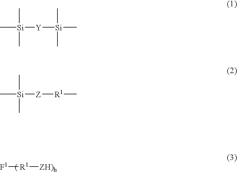
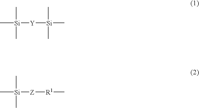
The present invention relates to an electrophotographic photoreceptor comprising a conductive support having formed thereon a specific photosensitive layer. The photosensitive layer comprises a siloxane resin-containing layer containing a siloxane resin having a structural unit represented by general formula (1) shown below, a structural unit represented by general formula (2) shown below, and an organic group derived from a compound having hole transport capability, or comprises a siloxane resin-containing layer containing a siloxane resin obtained by using an organic silicon compound having a structural unit represented by general formula (1) shown below and a hydrolytic group, and a compound represented by general formula (3) shown below: The formulas are defined in the specification.

Description

FILED OF THE INVENTION[0001] The present invention relates to an electrophotographic photoreceptor and a method for producing the same. The invention also relates to an image forming apparatus and a process cartridge.RELATED ART OF THE INVENTION[0002] In image forming apparatus such as copiers, printers and facsimiles, electrophotographic systems in which charging, exposure, development, transfer, etc. are carried out using electrophotographic photoreceptors have been widely employed. In such image forming apparatus, demands for speeding up of image formation processes, improvement in image quality, miniaturization and prolonged life of the apparatus, reduction in production cost and running cost, etc. are increasingly growing. Further, with recent advances in computers and communication technology, digital systems and color image output systems have been applied also to the image forming apparatus.[0003] In view of such a background, improvement in electrophotographic properties an...

Claims


Application Information

Patent Timeline
Patent Type & Authority Applications(United States)
IPC IPC(8): G03G5/05G03G5/06G03G5/147
CPCG03G5/0514G03G5/0578G03G5/0614G03G5/14773
Inventor YAMADA, WATARUNUKADA, KATSUMIKOSEKI, KAZUHIROIWASAKI, MASAHIROYAMASHITA, TAKAYUKI
Owner FUJIFILM BUSINESS INNOVATION CORP
Learn More