Optical interconnection circuit among wavelength multiplexing chips, electro-optical device, and electronic apparatus

a technology of optical interconnection circuit and wavelength multiplexing chip, which is applied in the direction of waveguides, instruments, semiconductor lasers, etc., can solve the problems of complicated connections between optical parts, such as light emitting elements and light receiving elements, and the signal transmission speed substantially reaches its limi

a technology of optical interconnection circuit and wavelength multiplexing chip, which is applied in the direction of waveguides, instruments, semiconductor lasers, etc., can solve the problems of complicated connections between optical parts, such as light emitting elements and light receiving elements, and the signal transmission speed substantially reaches its limi

US20040264867A1Inactive Publication Date: 2004-12-30SEIKO EPSON CORP

Image

  • Optical interconnection circuit among wavelength multiplexing chips, electro-optical device, and electronic apparatus
  • Optical interconnection circuit among wavelength multiplexing chips, electro-optical device, and electronic apparatus
  • Optical interconnection circuit among wavelength multiplexing chips, electro-optical device, and electronic apparatus

Examples


Embodiment Construction

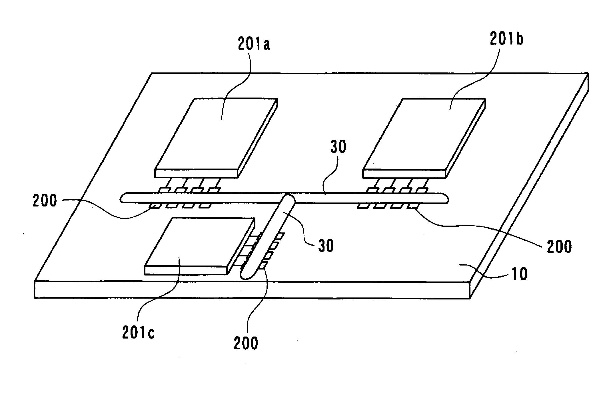
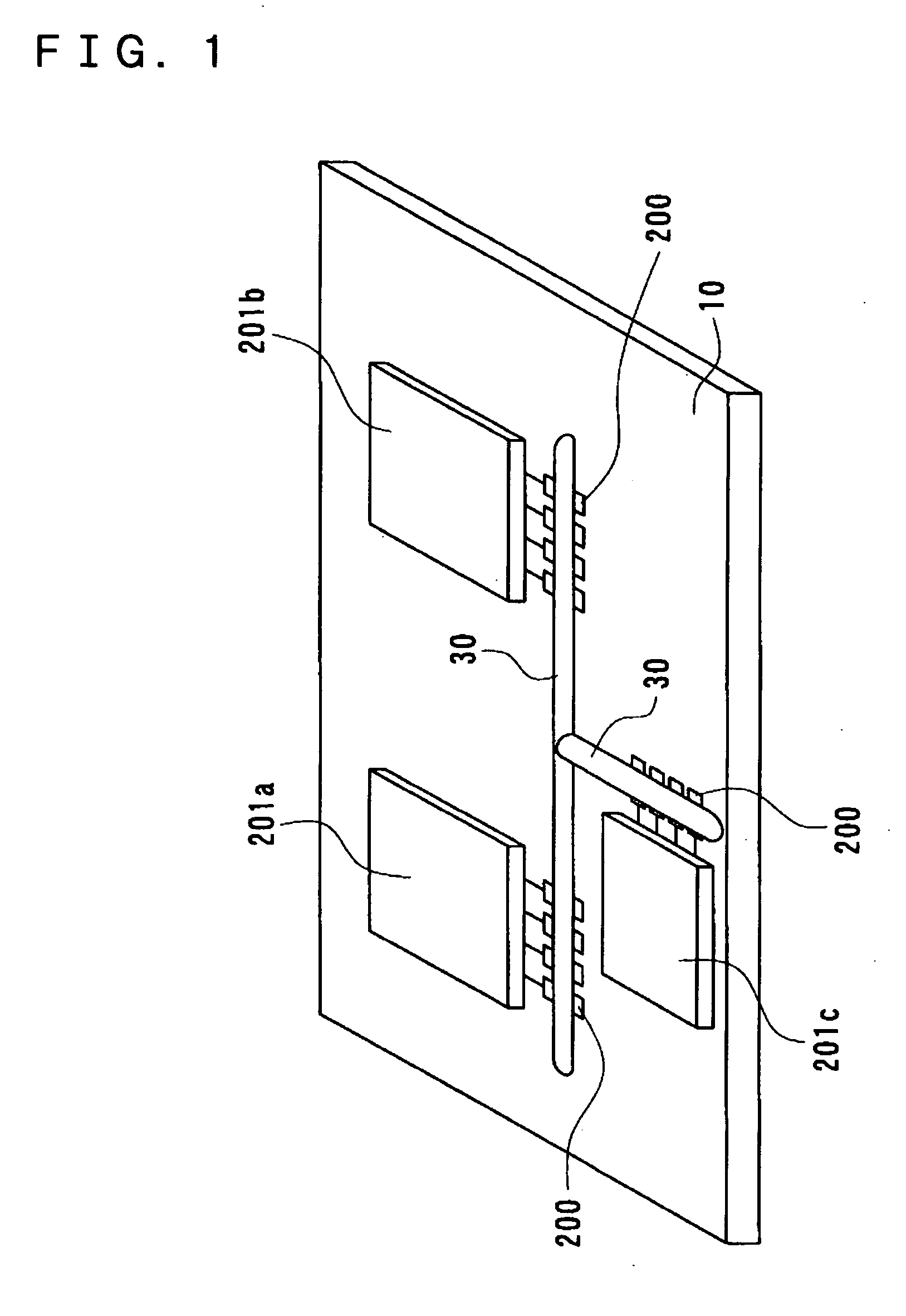
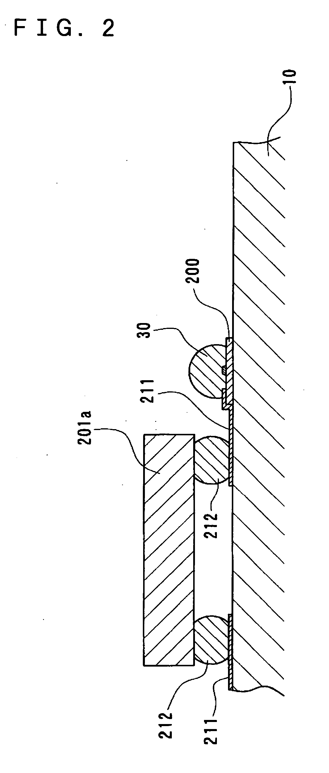
[0176] Hereinafter, an example of the application of the optical interconnection circuit among wavelength multiplexing chips according to an aspect of the present invention will be described.

[0177] For example, the on-chip optical interconnection circuits of the above-described exemplary embodiments are used as a signal transmission device of an optoelectronics integrated circuit system. A computer is used as the optoelectronics integrated circuit system. Next, integrated circuit chips constituting a CPU are formed on the substrate 10, and integrated circuit chips constituting a storage device are formed on the substrate 10. Although signal processing in the CPU and the storage device is performed using electrical signals, the optical interconnection circuit among wavelength multiplexing chips of the above-described exemplary embodiment is applied to the data transmission between IC chips.

[0178] As a result, in accordance with the present application in simple and easy configuration...


PUM


Abstract

To provide an optical interconnection circuit among wavelength multiplexing chips, capable of increasing signal transmission speed and of being easily made minute thereby being simply and easily fabricated, an electro-optical device, and an electronic apparatus, an optical interconnection circuit among wavelength multiplexing chips, which is disposed on a substrate, includes micro-tile shaped elements having a light emitting function or a light receiving function with wavelength selectivity.

Description

[0001] 1. Field of Invention[0002] The present invention relates to an optical interconnection circuit among wavelength multiplexing chips, an electro-optical device, and an electronic apparatus.[0003] 2. Description of Related Art[0004] Electro-luminescence panels (ELPs), plasma display panels (PDPs), and liquid crystal displays (LCDs) are recently used as plane display devices. In such plane display devices, a technology of using light to transmit signals is used in order to address the problem of signal delay caused by an increase in the sizes of the plane display devices and large capacity display.[0005] In computers, operation speed (an operation clock) inside CPUs increases year by year, as the internal structures of integrated circuits become minute. However, in buses to connect the CPUs to peripheral devices, such as memories, signal transmission speed substantially reaches its limit thereby becoming a bottleneck in the processing speed of computers. When optical signals are...

Claims


Application Information

Patent Timeline
30 Dec 2004
Publication
US20040264867A1
IPC
G02B6/122; G02B6/13; G02B6/42; G02B6/34; G02B6/43; G02F1/133; G02F1/1345; G02F1/135; G06F3/00; H01L21/60; H01L31/0232; H01L33/30; H01L33/48; H01L51/50; H01S5/022; H04B10/00; H04B10/275; H04B10/278; H04B10/524; H04B10/572; H04B10/80
CPC
G02B6/4214; G02B6/4246; H01L2224/1329; H01L2224/16227; H01L2224/133; H01L2224/131; H01L2224/82102; G02B6/43
Inventors
KONDO, TAKAYUKI