Semiconductor device fabrication method

a technology of semiconductor devices and fabrication methods, applied in semiconductor devices, semiconductor lasers, laser details, etc., can solve the problems of low yield, significant yield drop, monolithic integration, etc., and achieve the effect of convenient electrode formation

Inactive Publication Date: 2005-01-06
PANASONIC CORP
View PDF10 Cites 10 Cited by
  • Summary
  • Abstract
  • Description
  • Claims
  • Application Information

AI Technical Summary

Benefits of technology

[0038] When the semiconductor elements are the facet-emitting semiconductor laser elements, each of which emits a laser beam from a facet, the step (a) preferably includes a process in which a substrate electrode for contact with the periphery of the...

Problems solved by technology

Nevertheless, in the conventional monolithic two-wavelength laser diode array, active layers of the respective laser diodes have different compositions and thus have to be grown in different process steps, which results in the problem of low yields.
In particular, when high-output laser diodes are monolithically integrated, yields decrease significantly.
Moreover, it is very difficult, from the viewpoint of crystal growth, to monolithically integrate a gallium nitride (GaN)-based blue laser diode, which is used in high density DVDs, and an aluminum gallium indium phosphide (AlGaInP)-based ...

Method used


Image

  • Semiconductor device fabrication method
  • Semiconductor device fabrication method
  • Semiconductor device fabrication method

Examples


first embodiment

[0053] (First Embodiment)

[0054] Hereinafter, a first embodiment of the present invention will be described with reference to the accompanying drawings.

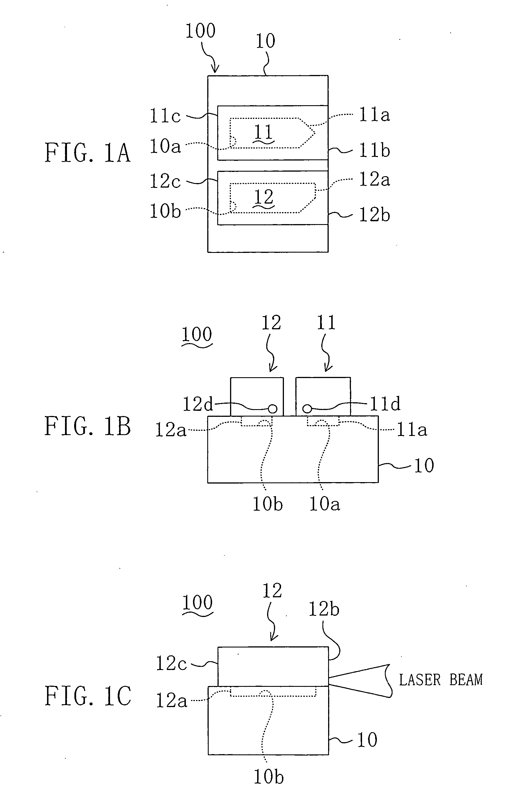
[0055]FIGS. 1A through 1C illustrate a semiconductor laser device in accordance with the first embodiment of the present invention. FIG. 1A shows a plan configuration, FIG. 1B shows a front configuration, and FIG. 1C shows a left-side configuration.

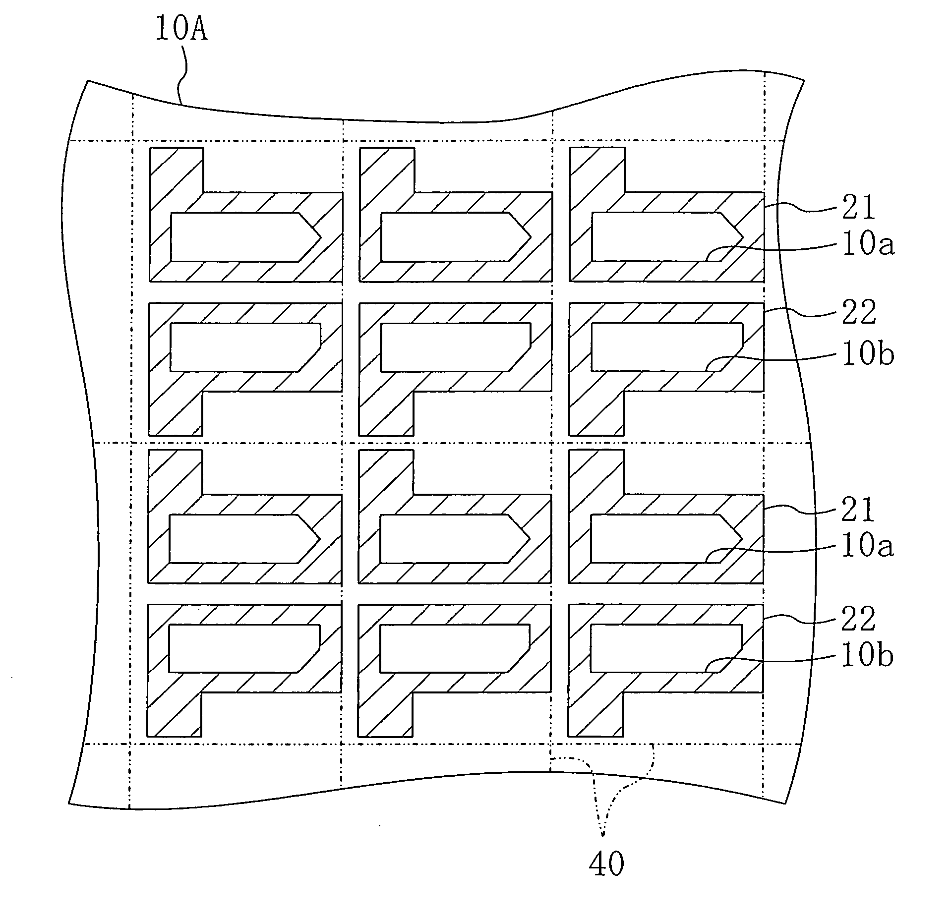
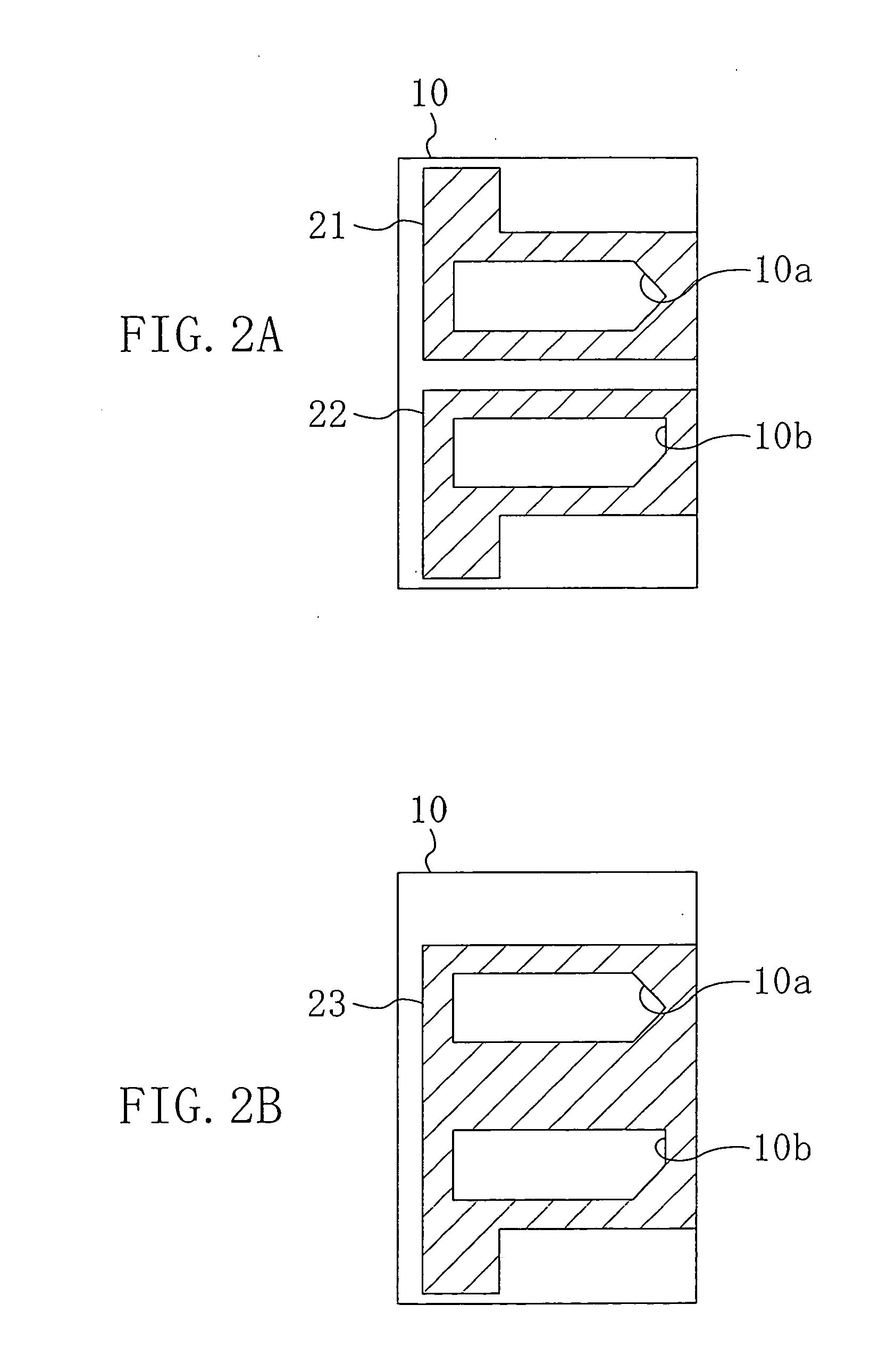
[0056] As shown in FIG. 1A, the semiconductor laser device 100 in accordance with the first embodiment includes a substrate 10, which is made of, e.g., silicon (Si) and which has first and second recessed portions 10a and 10b formed spaced apart from each other in the principal surface of the substrate 10.

[0057] Inserted in the first recessed portion 10a is a protruding portion 11a formed in the lower portion of a first semiconductor laser chip (semiconductor chip) 11 in the form of a function block, which emits, for example, an infrared laser beam. Inserted in the second recessed portio...

second embodiment

[0133] (Second Embodiment)

[0134] Hereinafter, a second embodiment of the present invention will be described with reference to the accompanying drawings.

[0135]FIGS. 12A through 12C illustrate a semiconductor laser device in accordance with the second embodiment of the present invention. FIG. 12A shows a plan configuration, FIG. 12B shows a front configuration, and FIG. 12C shows a left side configuration. In FIGS. 12A through 12C, the same members as those shown in FIGS. 1A thuough 1C are identified by the same reference numerals and the descriptions thereof will be omitted herein.

[0136] As shown in FIGS. 12A through 12C, a substrate 10B included in the semiconductor laser device 100 according to the second embodiment is characterized in that laser-beam-emitting facets 11b and 12b of semiconductor laser chips 11 and 12 are formed extending ahead of the front facet of the substrate 10B.

[0137] This prevents laser beams emitted by the respective semiconductor laser chips 11 and 12 f...


PUM


Abstract

In a semiconductor device fabrication method using a fluidic self-assembly technique in which in a liquid, a plurality of semiconductor elements are mounted in a self-aligned manner on a substrate with a plurality of recessed portions formed therein, protruding potions that are inserted in the respective recessed portions of the substrate are formed in the lower portions of the respective semiconductor elements, the liquid in which the semiconductor elements have been spread is poured over the substrate intermittently, and the substrate is rotated in a period of time in which the liquid is not poured.

Description

BACKGROUND OF THE INVENTION [0001] The present invention relates to methods for fabricating semiconductor devices, and more particularly relates to semiconductor device fabrication methods which enable semiconductor light emitters, such as semiconductor laser devices, to be mounted in a self-aligned manner. [0002] Typical digital-versatile-disc (hereinafter referred to as “DVD”) players and recorders need to have the capability of playing back not only DVDs but also compact discs (hereinafter referred to as “CDs”), and also have to include the capability of reproducing, and storing data on, recordable CDs (CD-Rs) which have become widespread rapidly in recent years. [0003] As light for reproducing DVDs, a red laser beam with a wavelength in the 650 nm band is employed, while an infrared laser beam with a wavelength in the 780 nm band is used as light for playing back CDs and CD-R discs. Thus, in the currently available DVD players and recorders, two semiconductor laser diodes are in...

Claims


Application Information

Patent Timeline
IPC IPC(8): H01S5/022H01L21/00H01L21/98
CPCH01L21/67121H01L2924/12041H01L25/50H01L2224/95085H01L2224/95136H01L2924/01002H01L2924/01004H01L2924/01013H01L2924/01015H01L2924/01016H01L2924/01049H01L2924/01078H01L2924/10329H01L2924/10349H01L2924/01005H01L2924/01006H01L2924/01033H01L24/95H01L2924/12042H01L2924/00
Inventor ONOZAWA, KAZUTOSHIUEDA, DAISUKETOJO, TOMOAKI
Owner PANASONIC CORP
Why Eureka
Try Eureka