Manufacturing method for wiring

a manufacturing method and technology for wiring, applied in vacuum evaporation coatings, chemical vapor deposition coatings, coatings, etc., can solve problems such as pattern defects, waste of about 90% of resists, and particularly serious problems, so as to improve quality and reduce space and efficiency of manufacturing lines , the effect of improving productivity

Inactive Publication Date: 2005-01-20
SEMICON ENERGY LAB CO LTD
View PDF15 Cites 88 Cited by
  • Summary
  • Abstract
  • Description
  • Claims
  • Application Information

AI Technical Summary

Benefits of technology

[0011] The present invention has been devised in view of such problems, and it is an object of the invention to provide a manufacturing method for wiring, a contact hole, and a display apparatus with a purpose of improving a through put and an efficiency in use of a material to reduce manufacturing cost by using an ink droplet jet method. In addition, it is an object of the invention to provide a manufacturing method for wiring, a contact hole, and a display apparatus, which can cope with an increase in size of a substrate, by using the plasma treatment method under the atmospheric pressure or a pressure close to the atmospheric pressure.
[0012] Moreover, it is an object of the invention to provide a semiconductor manufacturing apparatus that is capable of realizing a manufacturing method for wiring, a contact hole, and a display apparatus that solves the above-mentioned problems.

Problems solved by technology

However, despite the attempt, about 90% of the resist is wasted.
In the case in which a large substrate is used, such a problem is particularly serious.
Then, the resist at the ends is scraped off and adheres to the substrate at the time of handling the substrate, which leads to a pattern defect.
Further, when a thin film is formed on a substrate using a vacuum apparatus, a special apparatus or equipment for making the inside of a chamber vacuum is necessary, which increases manufacturing cost.
In the case in which a large substrate is used, since a size of the chamber is also increased inevitably, long treatment time is required to evacuate the inside of the chamber, and a large quantity of a film formation gas is also required.

Method used


Image

  • Manufacturing method for wiring
  • Manufacturing method for wiring
  • Manufacturing method for wiring

Examples


embodiment

[0051] (Embodiment Mode 1)

[0052] First, as a characteristic of the invention, plasma generating means, in which plural electrodes are arranged linearly, is used for scanning to perform etching treatment or ashing treatment under the atmospheric pressure or a pressure close to the atmospheric pressure (6.6×10²−1.1×10⁵ Pa). Thus, using FIGS. 1 and 2, an apparatus having plural cylindrical electrodes, in which a first electrode surrounds a second electrode and have nozzle-like narrow ports at tips thereof, will be explained as an example of a plasma treatment apparatus used in the present invention.

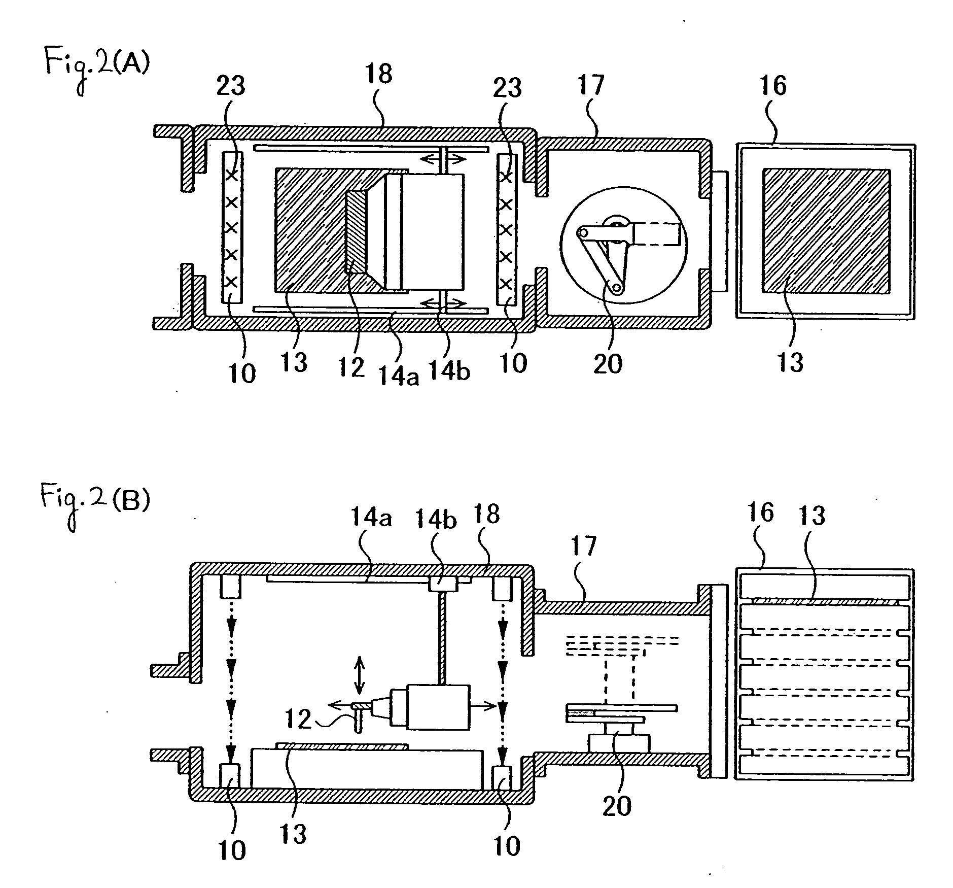
[0053]FIG. 2(A) is a top view of the apparatus, and FIG. 2(B) is a sectional view of the apparatus. In the figures, an object to be treated 13 such as a glass substrate and a resin substrate, which is represented by a plastic substrate with a desired size, is set in a cassette chamber 16. As a conveying system for the representative object to be treated 13, there is horizontal conveyance. H...

embodiments

[0119] (Embodiments)

[0120] [Embodiment 1]

[0121] Embodiments of the invention will be explained using the drawings.

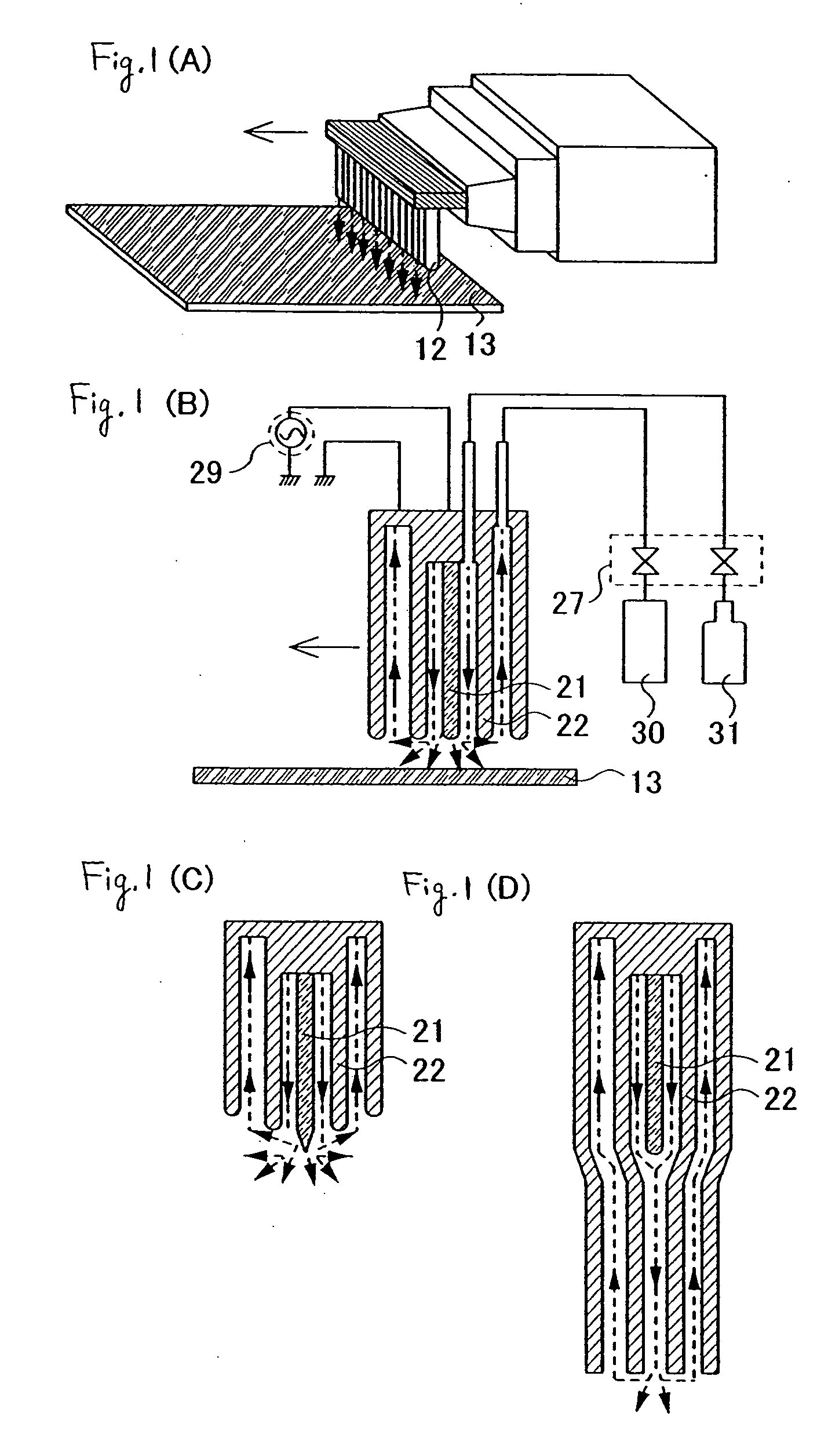
[0122]FIG. 7 shows an ink droplet jet apparatus using an ink droplet jet method. When a predetermined resist pattern is formed on a substrate 215 using the apparatus, a period for jetting a compound from a head (ink head) 201 and a moving speed of the substrate 215 are adjusted. Note that a nozzle 202, which blows out a gas, may be provided adjacent to the head 201, as smoothing means for a compound. The compound jetted on the substrate 215 is smoothed by the gas blown out from this nozzle 202. In other words, the head 201 or the substrate 215 is moved while keeping a distance between the head 201 and the substrate 215, whereby a linear pattern is formed. At this point, the pattern can be smoothed by blowing out the air from the nozzle 202. In addition, in order to improve accuracy of a position of impact of the jetted compound, it is preferable to bring a space between...

embodiment 2

[0135] [Embodiment 2]

[0136] An embodiment of the invention will be explained using the drawings.

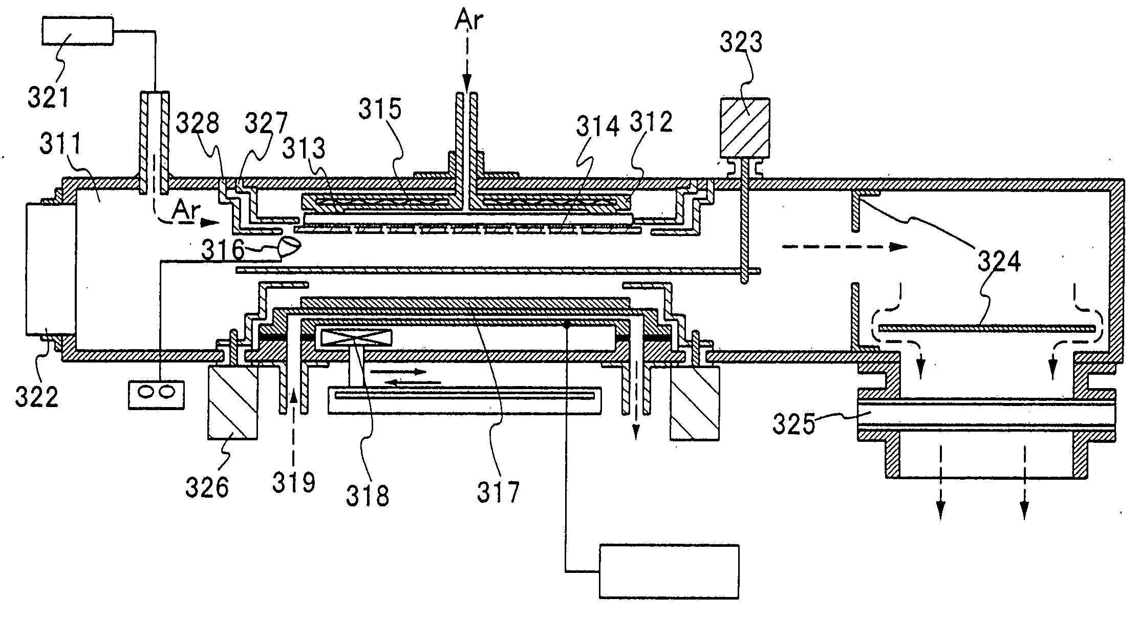
[0137]FIG. 9 is shows an example of a sputtering apparatus of a magnetron system. The apparatus has a film formation chamber 311 including a conveyance port (extraction port) 322 for extracting an object to be treated (substrate). A target 317 is provided in the film formation chamber 311 and is cooled (water-cooled) by a coolant 319 via a backing plate. A permanent magnet 318 makes it possible to form a film with high uniformity of thickness on a surface of a substrate opposed thereto by taking a circular motion or a linear motion in a direction parallel with a target surface. A shutter 323 opens and closes before and after starting film formation to prevent a film from being formed in a state in which plasma is unstable in an initial period of discharge.

[0138] A substrate 313 and a mask 314 are set in substrate holding means 312 by moving a substrate holder 327 and a mask holder 328. ...


PUM

PropertyMeasurementUnit
sizeaaaaaaaaaa
thicknessaaaaaaaaaa
frequencyaaaaaaaaaa

Abstract

In the case in which a film for a resist is formed by spin coating, there is a resist material to be wasted, and the process of edge cleaning is added as required. Further, when a thin film is formed on a substrate using a vacuum apparatus, a special apparatus or equipment to evacuate the inside of a chamber vacuum is necessary, which increases manufacturing cost. The invention is characterized by including: a step of forming conductive layers on a substrate having a dielectric surface in a selective manner with a CVD method, an evaporation method, or a sputtering method; a step of discharging a compound to form resist masks so as to come into contact with the conductive layer; a step of etching the conductive layers with plasma generating means using the resist masks under the atmospheric pressure or a pressure close to the atmospheric pressure; and a step of ashing the resist masks with the plasma generating means under the atmospheric pressure or a pressure close to the atmospheric pressure. With the above-mentioned characteristics, efficiency in use of a material is improved, and a reduction in manufacturing cost is realized.

Description

BACKGROUND OF THE INVENTION [0001] 1. Field of the Invention [0002] The present invention relates to a manufacturing method for wiring, a contact hole, and a display apparatus, and more specifically, to a manufacturing method for wiring, a contact hole, and a display apparatus that uses any one of a manufacturing method for a thin film such as a registration pattern using an ink droplet jet method (an ink jet method, an ink droplet discharge method), a manufacturing method for a thin film by a CVD (chemical vapor deposition) method, an evaporation method, or a sputtering method, and a local etching treatment method or ashing treatment method that is performed under the atmospheric pressure or a pressure close to the atmospheric pressure. In addition, the invention relates to a semiconductor manufacturing apparatus for forming a thin film. [0003] 2. Background Art [0004] A thin film transistor (TFT), which is formed using a thin film on an insulating surface, is widely applied for an...

Claims


Application Information

Patent Timeline
Patent Type & Authority Applications(United States)
IPC IPC(8): C23C16/44C23C16/455C23C16/509C23C16/54H01L21/285H01L21/312H01L21/3213H01L21/768H01L27/32H01L51/00H01L51/40H01L51/52
CPCC23C16/45589H01L27/124C23C16/54H01J2237/3342H01L21/2855H01L21/28562H01L21/312H01L21/32139H01L21/76802H01L21/76838H01L27/3246H01L51/0017H01L51/0022H01L51/5206H01L51/56H01L27/1288C23C16/509H10K59/122H10K71/231H10K71/611H10K50/81H10K71/00H01L21/02118
Inventor YAMAZAKI, SHUNPEIKUWABARA, HIDEAKI
Owner SEMICON ENERGY LAB CO LTD
Why Eureka
Try Eureka