Method of producing zinc oxide thin film, method of producing photovoltaic device and method of producing semiconductor device

a technology of photovoltaic devices and thin films, which is applied in the direction of pv power plants, light radiation electric generators, generators/motors, etc., can solve the problems of high cost of vacuum equipment, and insufficient light confinement effect at wavelengths of 600 to 1000 nm, etc., to achieve excellent optical properties, low material cost, and excellent optical properties

Inactive Publication Date: 2005-01-27
CANON KK
View PDF3 Cites 12 Cited by
  • Summary
  • Abstract
  • Description
  • Claims
  • Application Information

AI Technical Summary

Benefits of technology

[0025] (1-1) A method of producing a zinc oxide thin film comprising passing a current between a conductive substrate immersed in an aqueous solution containing at least zinc ions, ammonium ions, and zinc ammonia complex ions, and an electrode as an anode immersed in the aqueous solution to form a zinc oxide thin film on the conductive substrate. This producing method is capable of electrochemically forming a zinc oxide layer and forming an uneven surface which can sufficiently exhibit light confinement or light scattering for light at wavelength of 600 to 1000 nm. Therefore, it is possible to produce a photovoltaic device having high quality and low power cost. Particularly, the production cost of the zinc oxide layer can be decreased to about 1 / 100 of the sputtering method.
[0042] (3-6) A method of producing a photovoltaic device comprising the step of forming the zinc oxide thin film. This producing method is capable of stably forming the high-performance device at low cost.

Problems solved by technology

Although conventional known methods of producing a zinc oxide thin film include a vacuum deposition method, a sputtering method, an ion plating method, and a CVD method, all methods require an expensive vacuum apparatus, and an expensive vaporization source.
Also the light confinement effect at wavelengths of 600 to 1000 nm is insufficient.
However, in these wet methods, a substrate must be heated to about 300 to 800° C., and thus substrates which can be used are limited.
Also, zinc hydroxide is contained in the thin film together with zinc oxide, and it is thus difficult to form a pure zinc oxide thin film.
In these methods, since an expensive vacuum apparatus and expensive target are unnecessary, the production cost of a zinc oxide thin film can significantly be decreased.
However, the electrochemical deposition methods have the following problems:
(1) Particularly, an increase in current density or concentration of the solution causes the problem of easily producing abnormal growth of a needle-like, spherical, resin-like shape of the micron order or more on the deposited thin film.
The use of such a zinc oxide thin film as a part of a photovoltaic device possibly causes the abnormal growth to induce a shunt path in the photovoltaic device.
(2) In the zinc oxide thin film formed by one of the above methods, unevenness easily occurs in the grain sizes of zinc oxide crystals, and particularly, the problem of unevenness occurs in the case of a large area.
Conventionally, only smooth thin films are formed by the electrochemical deposition methods, and a method of electrochemically depositing a zinc oxide thin film having unevenness for the light confinement effect has not been established yet.

Method used


Image

  • Method of producing zinc oxide thin film, method of producing photovoltaic device and method of producing semiconductor device
  • Method of producing zinc oxide thin film, method of producing photovoltaic device and method of producing semiconductor device
  • Method of producing zinc oxide thin film, method of producing photovoltaic device and method of producing semiconductor device

Examples


example 1

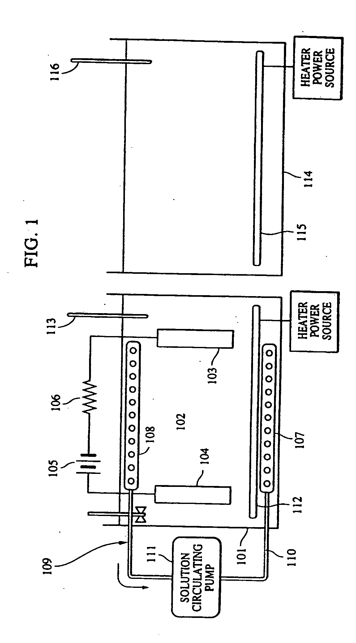
[0129] The zinc oxide thin film was produced by using the apparatus shown in FIG. 1.

[0130] As the conductive substrate 103 on the cathode side, a substrate of stainless 430BA having a thickness of 0.15 mm, and comprising Ag deposited to 300 nm by sputtering, with the back covered with an insulating tape (not shown in the drawing), was used. As the counter electrode 104 on the anode side, 4-N zinc having a thickness of 1 mm was used. The aqueous solution 102 was an aqueous solution of 0.03 mol / l zinc hydroxide in 10% ammonia at 65° C. and a pH of 10.3. The applied current was 1.0 mA / cm2 (0.1 A / dm2).

[0131] The thus-obtained electrodeposited film was examined by X-ray diffraction, and the deposition rate and reflectance at a wavelength of 800 nm were measured from optical-characteristics. The results are shown in Table 1.

TABLE 1Type of electrodeposited filmZinc oxideDeposition rate (μm / h)2Reflectance (%)90

[0132] The above results indicate that an excellent zinc oxide thin film can ...

example 2

[0133] Electrodeposition was carried out by the same method as Example 1 except that as the conductive substrate 103, a substrate of stainless 430BA having a thickness of 0.15 mm, and comprising Ag deposited to 100 nm by sputtering and zinc oxide deposited to 100 nm on Ag by sputtering, with the back covered with an insulating tape (not shown in the drawing), was used.

[0134] The thus-obtained electrodeposited film was examined by X-ray diffraction, and the deposition rate and reflectance at a wavelength of 800 nm were measured from optical characteristics. The results are shown in Table 2.

TABLE 2Type of electrodeposited filmZinc oxideDeposition rate (μm / h)3Reflectance (%)72

[0135] The above results indicate that an excellent zinc oxide thin film can be obtained by the method of producing a zinc oxide thin film of the present invention.

example 3

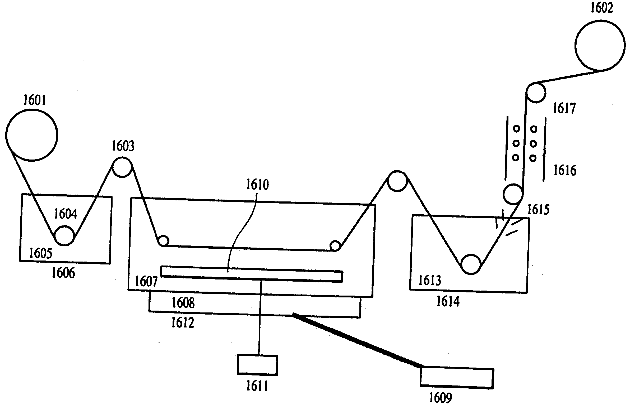
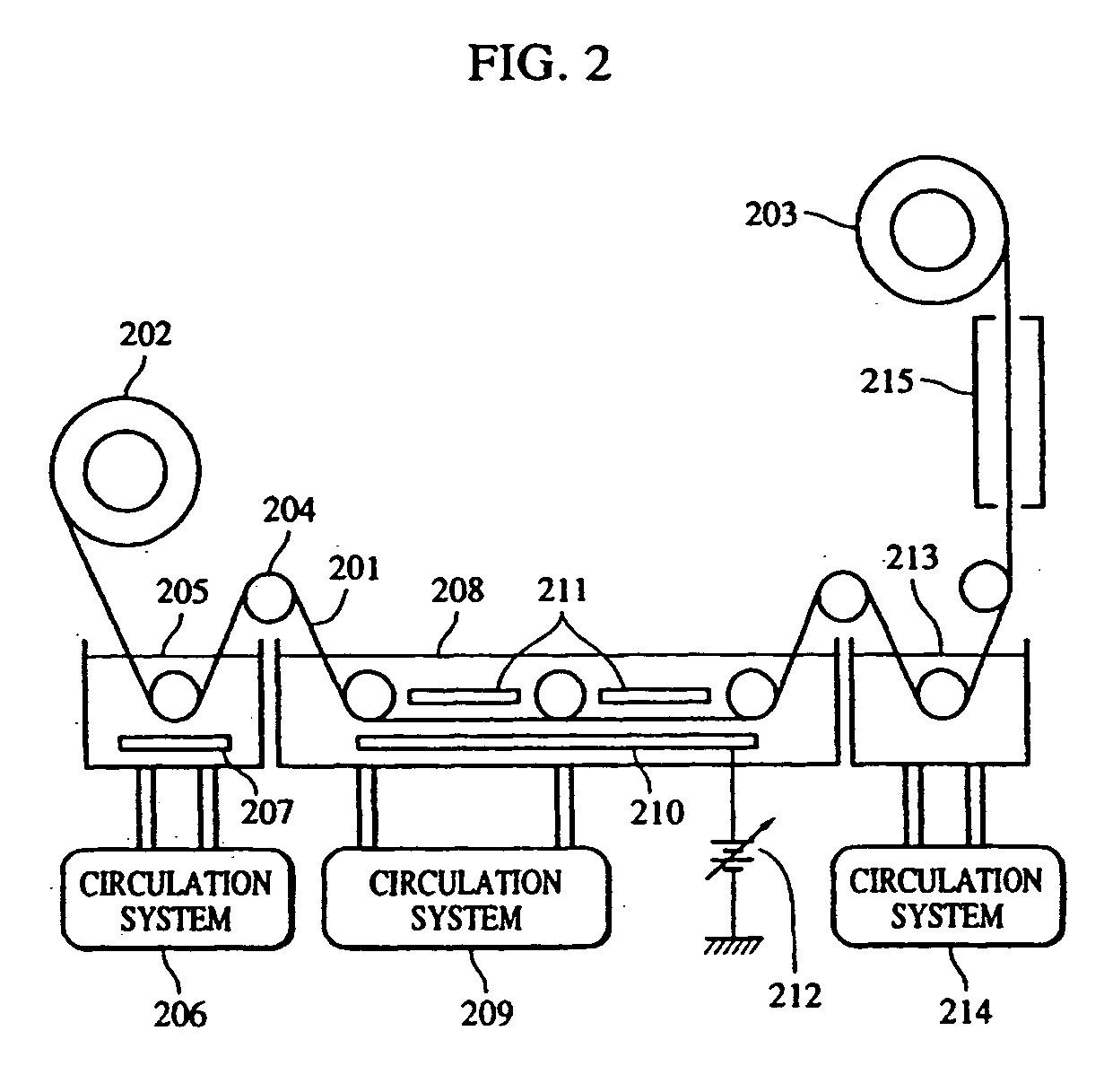
[0136] The solar cell shown in FIG. 3 and having a semiconductor layer having three p-i-n junctions, as shown in FIG. 4, was produced.

[0137] Specifically, the solar cell comprised the support 301-1 (conductive substrate of stainless steel SUS430, 10×10 cm2, thickness 0.2 mm), the metal layer 301-2 (Al), the transparent conductive layer 301-3 (zinc oxide thin film), the zinc oxide layer 302, the semiconductor layer 303, the transparent conductive layer 304, and the collecting electrodes 305 (Cu wire / Ag / C).

[0138] The metal layer 301-2 and the transparent conductive layer 301-3 were formed by the general vacuum deposition or sputtering method.

[0139] The zinc oxide layer 302 was formed by the same method as Example 1 except that 3 g / l of sucrose was added to the aqueous solution.

[0140] The semiconductor layer 303 was formed under the conditions shown in Table 3.

TABLE 3DepositionFormingtemperatureThicknessSemiconductor layermethod(° C.)(μm)First doped layer n-type a-Si:H:PRFCVD3000...


PUM

PropertyMeasurementUnit
pHaaaaaaaaaa
pHaaaaaaaaaa
pHaaaaaaaaaa

Abstract

The present invention provides a method of producing a zinc oxide thin film in which a current is passed between a conductive substrate immersed in an aqueous solution containing at least zinc ions, ammonium ions and zinc ammonia complex ions, and an electrode as an anode immersed in the aqueous solution to form a zinc oxide thin film on the conductive substrate. This method stabilizes formation of the zinc oxide thin film and improves adhesion between the thin film and the substrate.

Description

BACKGROUND OF THE INVENTION [0001] 1. Field of the Invention [0002] The present invention relates to a method of producing a zinc oxide thin film, a method of producing a photovoltaic device, and a method of producing a semiconductor device substrate. [0003] 2. Description of the Related Art [0004] In a conventional photovoltaic device comprising amorphous silicon hydride, amorphous silicon germanium hydride, amorphous silicon carbide hydride, microcrystalline silicon or polycrystalline silicon, a reflecting layer formed on the back thereof is utilized for improving a collection efficient at long wavelengths. Such a reflecting layer preferably exhibits effective reflection properties at a wavelength near the band ends of a semiconductor material at which absorption is low, i.e., a wavelength of 800 to 1200 nm. Materials satisfying this condition include metals such as gold, silver, copper and aluminum. [0005] Also, an uneven layer optically transparent in the predetermined wavelengt...

Claims


Application Information

Patent Timeline
Patent Type & Authority Applications(United States)
IPC IPC(8): C25D9/04C25D9/08C01G9/02H01L31/0216H01L31/0236H01L31/04
CPCC25D9/04Y02E10/50H01L31/0236H01L31/02167H01L31/02363
Inventor SANO, MASAFUMISONODA, YUICHI
Owner CANON KK
Why Eureka
Try Eureka