Oxygen-doped al-containing current blocking layers in active semiconductor devices in photonic integrated circuits (PICs)

a photonic integrated circuit and active semiconductor technology, applied in semiconductor devices, lasers, semiconductor lasers, etc., can solve the problems of limiting the high speed characteristics of such devices, reverse biased p-n junctions in these devices may possess leakage paths leading to high thresholds, and may not be readily adaptable to bit rate, etc., to achieve greater oxygen incorporation, prevent current flow, and improve control

Inactive Publication Date: 2005-02-24
INFINERA CORP
View PDF35 Cites 13 Cited by
  • Summary
  • Abstract
  • Description
  • Claims
  • Application Information

AI Technical Summary

Benefits of technology

[0014] Further, according to this invention, an Al containing group III-V compound semi-insulating layer is formed during MOCVD growth using an oxygen source to from a current blocking layer or region that defines a current channel or region in active semiconductor devices incorporated in a photonic integrated circuit (PIC), examples of such devices comprising buried heterostructure semiconductor lasers, LEDs, modulators, photodiodes, heterojunction bipolar transistors, field effect transistors or other active devices and for preventing current flow through designated regions of the device.
[0015] An important aspect of this invention is the provision of current blocking layers formed in such active semiconductor devices that are formed from intentional oxygen doping during their epitaxial growth. The deployment of intentional oxygen doping provides for better control and greater oxygen incorporation during layer growth over a wider range of growth parameters so that higher, repeatable resistivity values can be achieved under those conditions, such as 106-8 Ωcm or higher. These current blocking layers particularly contained Al and are lattice matched to the substrate, such as InAlGaP latticed matched to GaAs or InAlGaAs latticed matched to InP. The oxygen doping may be provided via an O2 flow into the MOCVD reactor or provided via an oxide source where the oxide is cracked, i.e., the oxygen is dissociated from other gas constituents. However, an oxide source is preferred over an O2 gas source because the latter provides a higher cracking temperature and reduced pre-reactions as described earlier. The preferred source for intentional oxygen doping is with a low vapor pressure oxide source such as, for example, a nitrogenous oxide (NOx) or dialkylaluminum aloxides or diethyl aluminum alkoxide (DEALO). An ideal oxygen source is one that has a low cracking temperature without any tendency of pre-acting in the reactor with other source constituents prior to epitaxial wafer deposition. The material regime of particular interest is InAlAs / InP for achieving wavelengths of interest in optical telecommunication systems. Instead of InAlAs:O as a blocking layer material, InAlGaAs:O or AlGaAsSb:O or alternating layers of or alternating monolayers of AlAs:O / InAs or AlGaAs:O / InAs or InAlGaAs:O / InAs may be utilized or substitute InGaAs, InAlAs, InGaAsP for any of the InAs layers here. Also, combinations of the ternary layers and the quaternary layers may be employed, such as alternating layers of InAlAs:O and InAlGaAs:O. In the case of all the embodiments disclosed in this application, Fe can be co-doped with O since the oxygen at donor sites provides a strong holding bond for the out-diffusion of Fe from the material as well as prevention of the in-diffusion of other dopants, such as Zn, into the formed current blocking layer. Furthermore, O-doped layers can bond other layers with mobile elements (e.g., Fe) to prevent the indiffusion or out-diffusion of impurities into or out of these layers.
[0017] To enhance the effect of oxygen doping of the Al-III-V current blocking layer or region and the resulting resistivity level, the Al content in the deposited layer is preferably 0.5 mole fraction or greater.

Problems solved by technology

However, due to intrinsic capacitance, these types of blocking junctions may not be readily adaptable for bit rates higher than 2.5 Gb / s.
The particular problem with respect to these types of blocking layers is that the reverse biased p-n blocking junction possess a significant junction capacitance, limiting the high speed characteristics of such devices.
Also, the reverse biased p-n junction in these devices may possess leakage paths leading to high thresholds in the case of laser diodes as well as low quantum efficiencies in all such devices.
The use of Fe doped Group III-V blocking layers is a well established current blocking technology but plagued by problems.
In particular, Fe doped layers have poor stability so that Fe readily diffuses into adjacent semiconductor layers or materials, particularly the active region of a device.
The dependence on background doping levels in a reactor or other growth apparatus to achieve a desired level of resistivity is a difficult approach to form current blocking layers having uniform characteristics on continuous and repeatable fabrication basis.
As a result, background doping levels can substantially vary from reactor run to reactor run, resulting in significant variations in the current blocking properties of the compounds and materials formed when utilizing this technique and approach.
As previously indicated relative to U.S. Pat. No. 5,804,840, SI-InAlAs, via low growth temperatures and background impurities, does not provide sufficiently high resistive values or well controlled active semiconductor devices employed particularly in optical telecommunication applications where the active semiconductor devices are integrated as a photonic integrated circuit (PIC) with close device spacing encountered so that the highest achievable levels of low current leakage in such devices are required, e.g., resistivities in a range of about 106 to 108 Ωcm or more.
As indicated earlier, this large range is not acceptable for current blocking applications in demanding applications.
Furthermore, using O2 as an oxygen source has the disadvantage of pre-reacting with the Group III-V growth source materials in the MOCVD reactor chamber.
These pre-reactions make the controlled incorporation of oxygen difficult and cause other detrimental problems such as undesired deposits in the reactor chamber and problems with composition or constituent control of the epitaxial deposition of Group III-V components comprising the compounds or layers that are being epitaxially grown in the reactor.

Method used


Image

  • Oxygen-doped al-containing current blocking layers in active semiconductor devices in photonic integrated circuits (PICs)
  • Oxygen-doped al-containing current blocking layers in active semiconductor devices in photonic integrated circuits (PICs)
  • Oxygen-doped al-containing current blocking layers in active semiconductor devices in photonic integrated circuits (PICs)

Examples


first embodiment

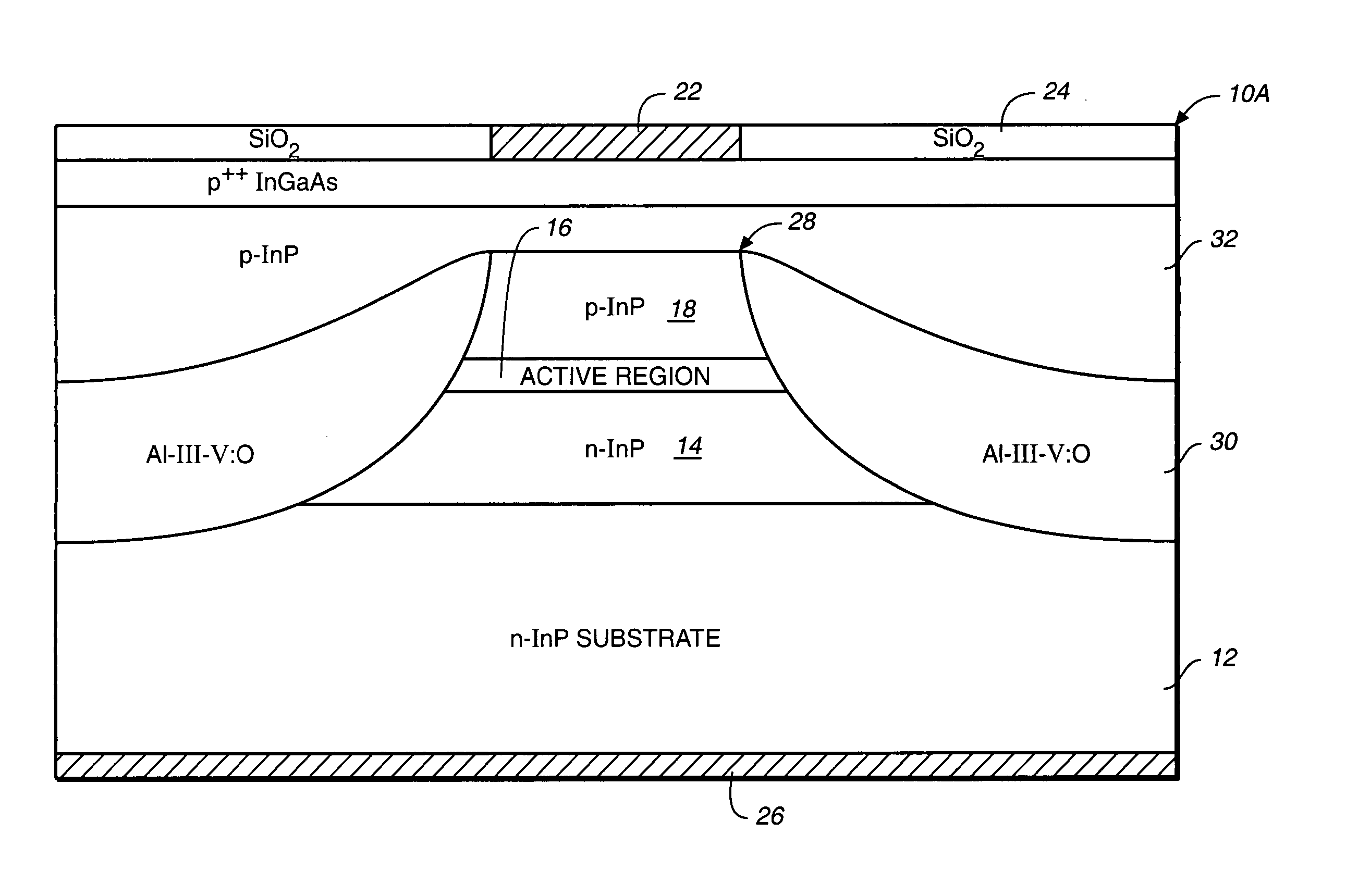
[0038] Reference is now made to FIG. 1 illustrating this invention in a generally generic form. Active semiconductor device 10A may be, for example, any such semiconductor device that is rendered operative through the establishment of a current channel through the device, such as, a semiconductor laser diode, semiconductor optical amplifier (SOA), LED or EA modulator, just to name a few such devices. Device 10A comprises a substrate 12, for example, n-InP, upon which is grown lattice-matched or pseudomorphic strained active layer or layers comprising active region 16. To provide for carrier recombination under applied bias conditions, Group III-V epitaxially grown layers may be provided with an n-type dopant, such as Si or S, or with a p-type dopant such as Zn or Mg, as is well known in the art. Substrate 12 could also be GaAs but for wavelengths useful in present optical telecommunication systems, the preferable material system for these devices are InP material systems, such as, b...

second embodiment

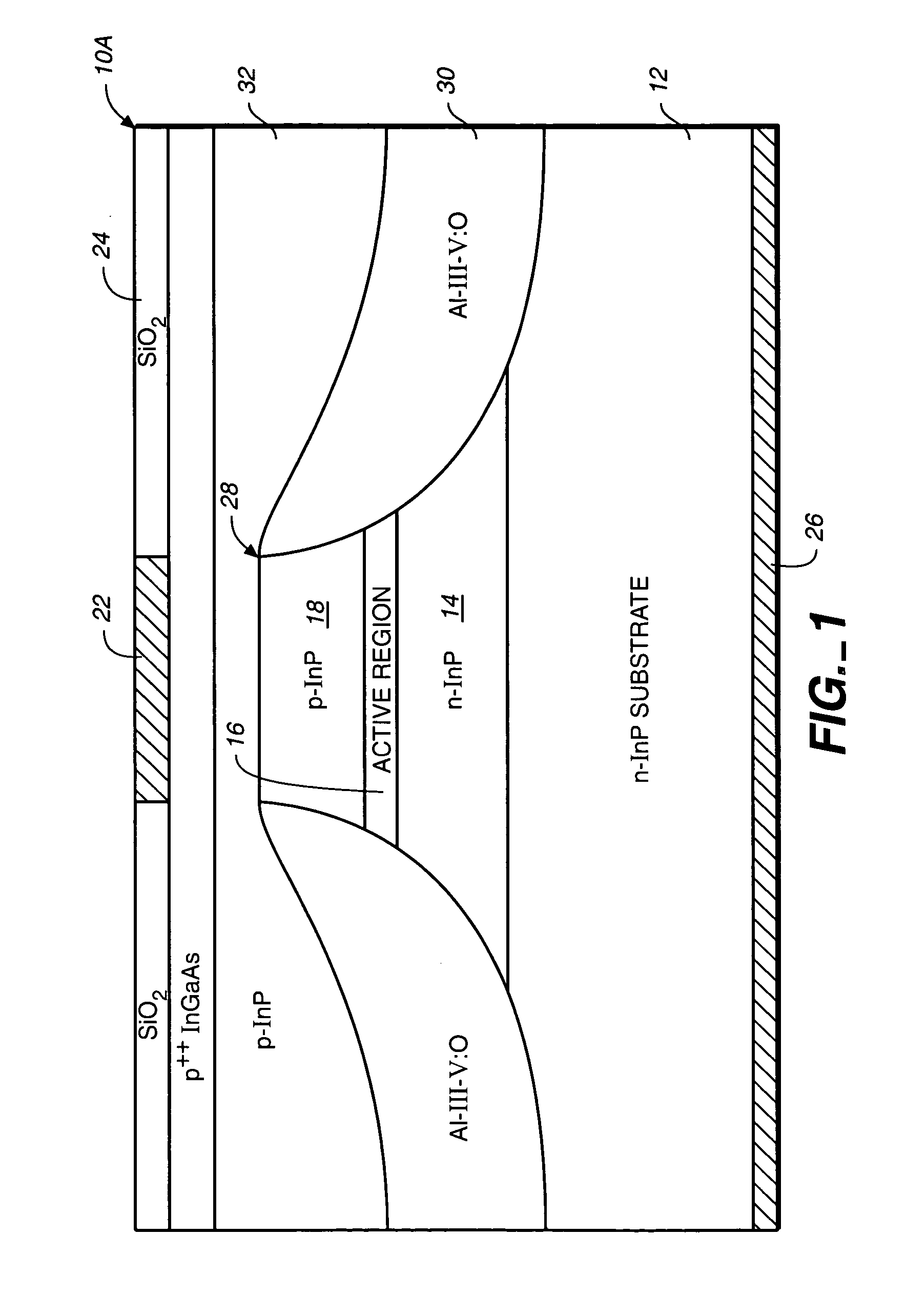
[0045] Reference is now made to FIG. 2 which discloses this invention. In this embodiment as well as in all subsequent embodiments, the previous description relative to elements and components in FIG. 1 equally apply to all of the same elements and components having the same numerical identification in figures of the subsequent embodiments. FIG. 2 is the same as FIG. 1 except there is, in addition, the deposited layers 34 and 36 between which is formed current blocking Al-III-V layer30. These layers 34 and 46 are optionally added in the case where, for example, the close proximity of the Al-III-V:O layer to the mesa 28 or active region 16 may induce deleterious device effects (e.g., high interface recombination). In these cases, it may be desirable to set-back the Al-III-V:O layer with a layer of InP or InP:O. This layer should be in the range of about 100 Å to 2 μm thick, preferably about 500 Å to 5,000 Å thick. In the case of layer 34, this lower set-back layer may comprise InP, I...

third embodiment

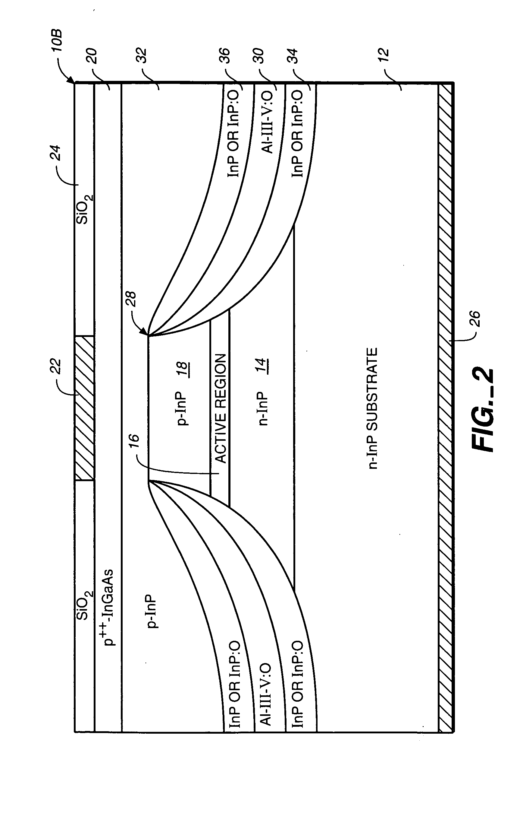
[0046] Reference is made to FIG. 3 illustrating this invention comprising the same layers as shown in FIG. 2 except that here, the material of choice for current blocking layer 30 is InAlAs:O sandwiched between layers 34A and 36A of n-InP and p- or n-InP, respectively. Alternatively, layer 36A can be doped as InP:O. While InAlAs:O is illustrated in this embodiment for blocking layer 30, it should be understood that blocking layer 30 may also be InAlGaAs:O or alternating layers or monolayers of AlAs:O / InAs, the latter of which will be described in more detail later, such as relative to the embodiment shown in FIG. 6.


PUM


Abstract

In photonic integrated circuits (PICs) having at least one active semiconductor device, such as, a buried heterostructure semiconductor laser, LED, modulator, photodiode, heterojunction bipolar transistor, field effect transistor or other active device, a plurality of semiconductor layers are formed on a substrate with one of the layers being an active region. A current channel is formed through this active region defined by current blocking layers formed on adjacent sides of a designated active region channel where the blocking layers substantially confine the current through the channel. The blocking layers are characterized by being an aluminum-containing Group III-V compound, i.e., an Al-III-V layer, intentionally doped with oxygen from an oxide source. Also, wet oxide process or a deposited oxide source may be used to laterally form a native oxide of the Al-III-V layer. An example of a material system for this invention useful at optical telecommunication wavelengths is InGaAsP / InP where the Al-III-V layer comprises InAlAs:O or InAlAs:O:Fe. Other materials for the blocking layers may be InAlGaAs or alternating layers or alternating monolayers of AlAs / InAs. Thus, the O-doped blocking layers may be undoped, impurity doped or co-doped with Fe.

Description

REFERENCE TO RELATED APPLICATION [0001] This application is continuation of nonprovisional patent application, Serial No. 10 / 319,962, filed Dec. 16, 2002 and entitled, OXYGEN-DOPED Al-CONTAINING CURRENT BLOCKING LAYERS IN ACTIVE SEMICONDUCTOR DEVICES and published on Dec. 25, 2003 as Pub. No. 2003 / 0234969 and claiming priority of provisional patent application Serial No. 60 / 340,319, filed Dec. 14, 2001; and nonprovisional patent application Ser. No. 10 / 267,331, filed Oct. 8, 2002 and entitled, TRANSMITTER PHOTONIC INTEGRATED CIRCUITS (TxPIC) AND OPTICAL TRANSPORT NETWORKS EMPLOYING TxPICs and published on May 22, 2003 as Pub. No. 2003 / 0095737 and claiming priority of provisional patent application Ser. No. 60 / 328,207, filed Oct. 9, 2001, all which patent applications are incorporated herein by their reference.BACKGROUND OF THE INVENTION [0002] 1. Field of the Invention. [0003] This invention relates generally to active semiconductor devices, such as photonic, electronic or optoelect...

Claims


Application Information

Patent Timeline
Patent Type & Authority Applications(United States)
IPC IPC(8): H01L29/165H01L29/22H01L29/40H01L31/0304H01L31/109H01L31/153H01L33/14H01S5/00H01S5/026H01S5/20H01S5/22H01S5/223H01S5/227H01S5/343
CPCB82Y20/00Y02E10/544H01L31/109H01L33/145H01S5/026H01S5/2072H01S5/221H01S5/2224H01S5/2226H01S5/2227H01S5/2231H01S5/227H01S5/2275H01S5/3072H01S5/34306H01L31/03046
Inventor KISH, FRED A. JR.MATHIS, SHEILA K.JOYNER, CHARLES H.SCHNEIDER, RICHARD P.
Owner INFINERA CORP
Why Eureka
Try Eureka