High temperature attachment of organic molecules to substrates

a technology of organic molecules and substrates, applied in the field of semiconductor fabrication, can solve the problems of degrading organic molecules and producing fairly toxic materials, and achieve the effect of enhancing the integration of molecular materials and completing in short tim

Inactive Publication Date: 2005-03-03
RGT UNIV OF CALIFORNIA
View PDF20 Cites 45 Cited by
  • Summary
  • Abstract
  • Description
  • Claims
  • Application Information

AI Technical Summary

Benefits of technology

This Invention provides a new procedure for attaching molecules to semiconductor surfaces, in particular silicon. The molecules include porphyrins and ferrocenes, which have been previously shown to be attractive candidates for molecular-based information storage. The new attachment procedure is simple, can be completed in short times, requires minimal amounts of material, is compatible with diverse molecular functional groups, and in some instances affords unprecedented attachment motifs. These features greatly enhance the integration of the molecular materials into the processing steps that are needed to create hybrid molecular / semiconductor information storage devices.

Problems solved by technology

Such approaches, however, have typically involved difficult reaction conditions, have been relatively inefficient, have degraded the organic molecule(s), and / or have resulted in the production of fairly toxic materials.

Method used


Image

  • High temperature attachment of organic molecules to substrates
  • High temperature attachment of organic molecules to substrates
  • High temperature attachment of organic molecules to substrates

Examples


example 1

Molecules Can Perform in Electronic Devices Under Real-World Processing and Operating Conditions

The central tenet of the field of molecular electronics is that molecular components can be used as functional elements in place of the semiconductor-based devices present in conventional microcircuitry (Kwok and Ellenbogen (2002) Materials Today, 28-37; Carroll and Gorman (2002) Angew. Chem. Int. Ed. 41: 4378-4400). To serve in this role, the molecular components should remain robust under daunting conditions including high-temperature (e.g., 400 ° C.) processing steps during manufacture and very large numbers (109-1012) of operational cycles over a lifetime (International Technology Roadmap for Semiconductors (ITRS), Semiconductor Industry Association, San Jose, Calif. (2000)). There has been considerable skepticism whether molecular materials possess adequate stability to meet such requirements. Herein, we demonstrate that porphyrin-based information storage media meet the processing...

example 2

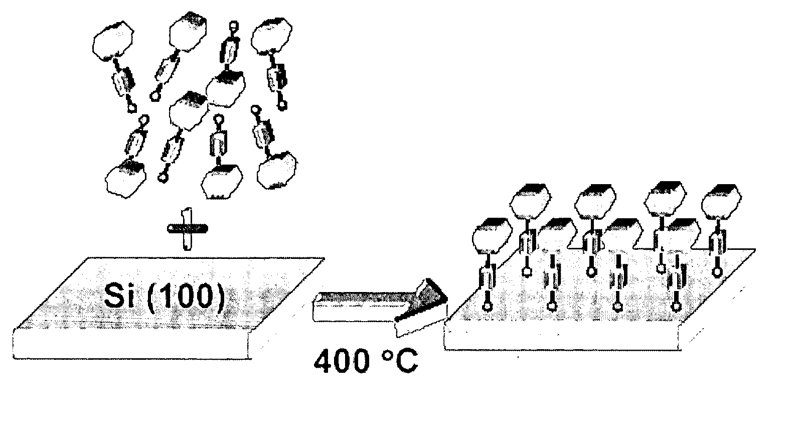
Solvent Free Attachment

FIG. 7 illustrates an experimental set-up that was used to prove the concept of gas phase molecular attachment. As illustrated in panel (a), we put a drop of molecular solution (redox-active porphyrin in tetrahydrofuran, (THF) solvent) on top of a piece of silicon wafer in a vial. A second piece of silicon wafer was placed next to it. We then sealed the vial and purged it with argon for several minutes to remove / dry THF. This leaves only a molecule powder on the first silicon piece. During the purge, the argon flow was kept low so that no molecule powder would be blown to the other silicon chip. After this step, the vials were heated at various temperatures (300-400 ° C. for 10-20 min). Afterwards the vials were cooled down to room temperature, and the silicon pieces were rinsed with dichloromethane.

A second set-up is illustrated in FIG. 7 (panel b), where no solvent was involved. We sealed the powder comprising the molecule together with a silicon piece in...

example 3

Facile Covalent Attachment of Porphyrins to Semiconductor Surfaces via High Temperature Processes

The field of molecular electronics has been driven by the prospect that devices that rely on the bulk properties of semiconductors will fail to retain the required characteristics to function when feature sizes reach nanoscale dimensions. As a consequence, there has been much interest in developing molecular-based electronic materials for use in both memory architectures and circuit elements (see, e.g., Kwok et al. Materials Today (February 2002), 28-37; Carroll and Gorman (2002) Angew. Chem. Int. Ed., 41: 4378-4400). Towards this goal, we have been engaged in a program aimed at constructing devices that use the properties of molecules to store information (Roth et al. (2000) Vac. Sci. Technol. B 18: 2359-2364; Roth et al. (2003) ACS Symp. Series, 844: 51-61; Roth et al. (2003) Am. Chem. Soc., 125: 505-517; Li et al. (2002) Appl Phys. Lett., 81: 1494-1496; Li et al. (2003) Appl. Phys. ...


PUM

PropertyMeasurementUnit
temperatureaaaaaaaaaa

Abstract

This invention provides a new procedure for attaching molecules to semiconductor surfaces, in particular silicon. The molecules, which include, but are not limited to porphyrins and ferrocenes, have been previously shown to be attractive candidates for molecular-based information storage. The new attachment procedure is simple, can be completed in short times, requires minimal amounts of material, is compatible with diverse molecular functional groups, and in some instances affords unprecedented attachment motifs. These features greatly enhance the integration of the molecular materials into the processing steps that are needed to create hybrid molecular / semiconductor information storage devices.

Description

FIELD OF THE INVENTION This invention pertains to the field of semiconductor fabrication. In particular this invention provides novel methods of coupling organic molecules to group III, IV, and V elements (e.g., silicon, germanium, etc.), and the like. BACKGROUND OF THE INVENTION The fabrication of ordered molecular assemblies on conducting silicon and other surfaces is of considerable interest owing to its potential applications in the microelectronic industry. One goal of semiconductor fabrication is to increase the density of active elements provided on an integrated circuit. In order to accomplish this, efforts have turned to the use of self-assembling molecular structures as an alternative to, or in conjunction with various lithographic processes to form the active elements used in integrated circuits. In addition, interest has turned to the use of organic molecules to form such active elements (e.g., memory elements) (see, e.g., U.S. Pat. Nos. 6,272,038, 6,212,093, and 6,20...

Claims


Application Information

Patent Timeline
Patent Type & Authority Applications(United States)
IPC IPC(8): G11C13/02H01L21/477H01L51/00H01L51/30H01L51/40H01M4/60H01M14/00
CPCB82Y10/00G11C13/0014G11C13/0016H01L51/0002H01L51/0008H01L51/001Y02E10/549H01L51/0075H01L51/0077H01L51/0595H01L51/4213H01M4/60H01M14/005H01L51/0026G11B9/149G11B9/14Y02E60/10H10K71/10H10K71/16H10K71/164H10K71/40H10K85/701H10K85/30H10K10/701H10K30/10
Inventor BOCIAN, DAVID F.LINDSEY, JONATHANLIU, ZHIMINGYASSERI, AMIR A.MISRA, VEENZHAO, QIANLI, QILIANGSURTHI, SHYAMLOEWE, ROBERT S.
Owner RGT UNIV OF CALIFORNIA
Why Eureka
Try Eureka