Method for chemical etch control of noble metals in the presence of less noble metals
- Summary
- Abstract
- Description
- Claims
- Application Information
AI Technical Summary
Benefits of technology
Problems solved by technology
Method used
Image
Examples
Embodiment Construction
[0025] The present invention is related to U.S. patent application Ser. No. 10 / 086,117, filed on O2 / 26 / 2002 (Bojkov et al., “Waferlevel Method for Direct Bumping on Copper Pads in Integrated Circuits”).
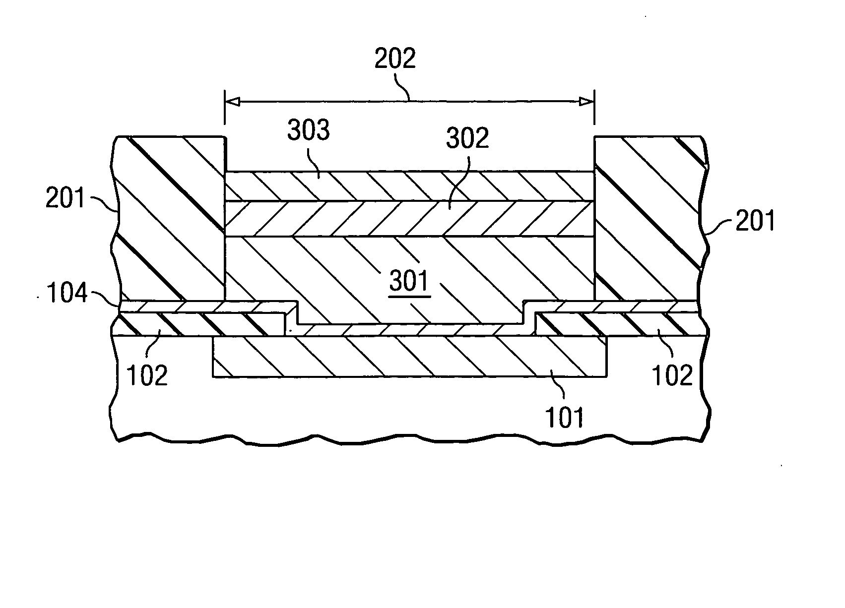
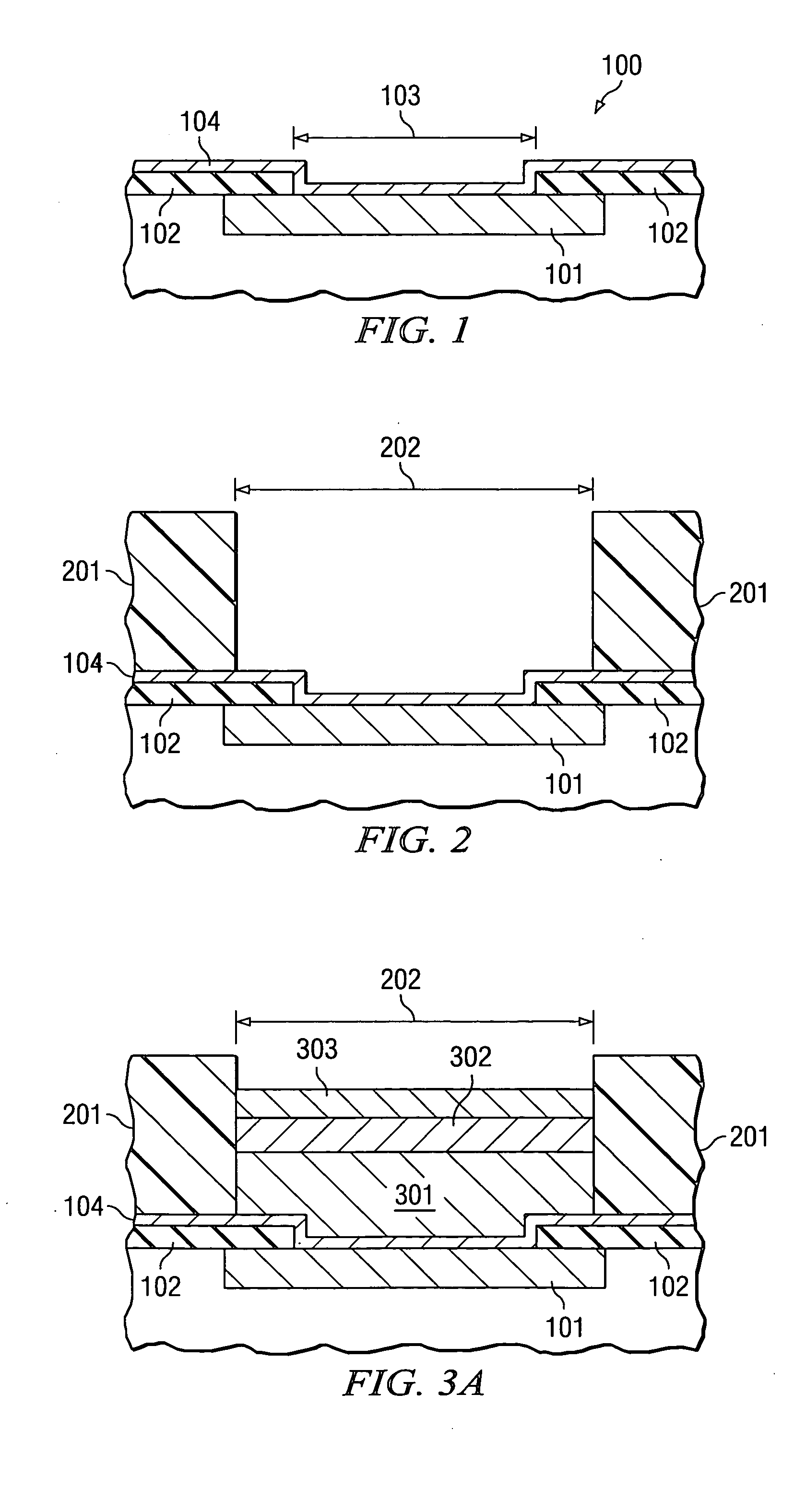
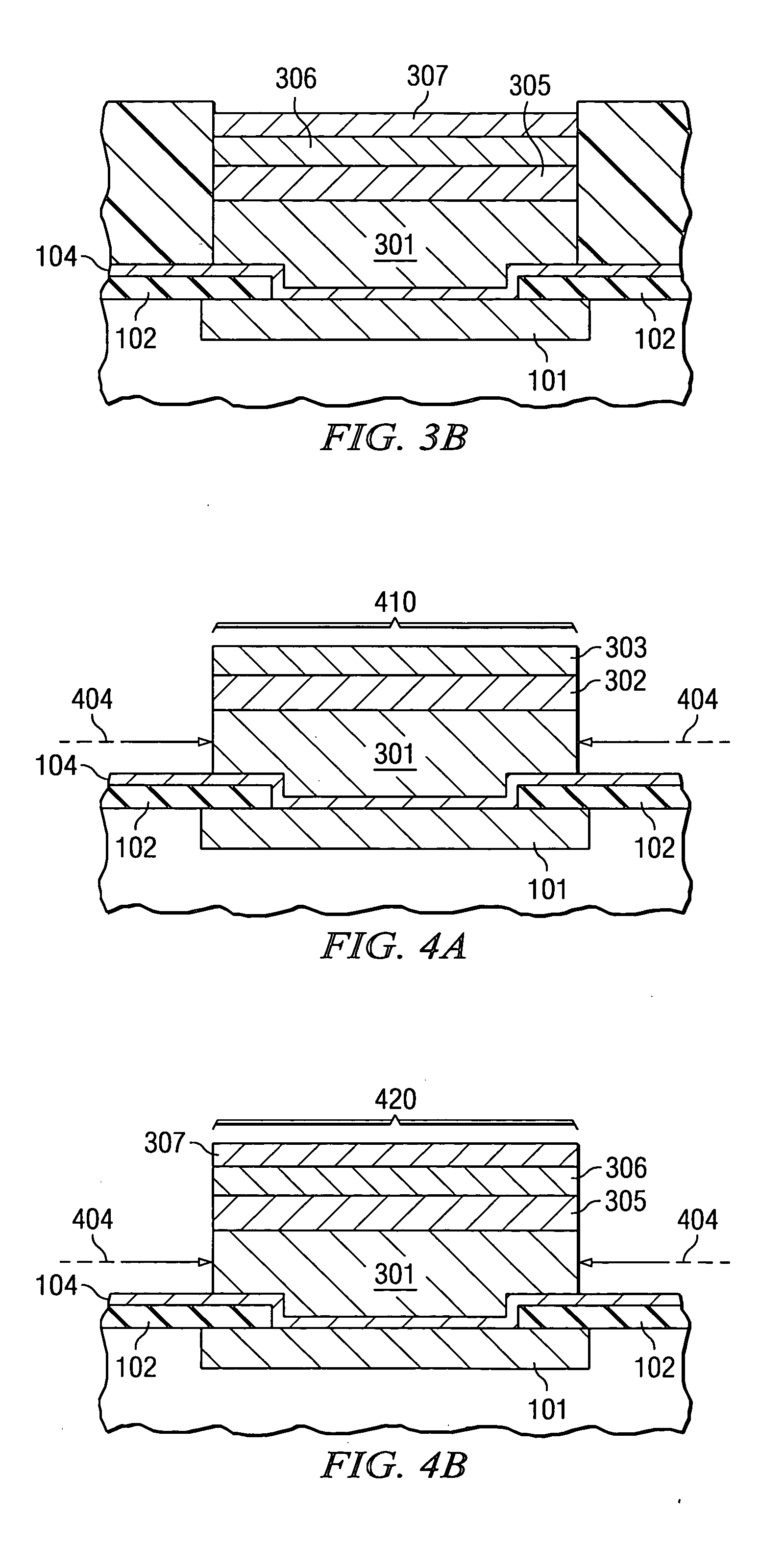
[0026] FIGS. 1 to 5B are schematic cross sections illustrating certain steps in the process flow for completing the fabrication of a bonding pad on an integrated circuit (IC) wafer. FIG. 1 shows schematically a portion of a semiconductor wafer, generally designated 100, having interconnections 101 and a protective overcoat 102. The semiconductor material is preferably silicon, but may alternatively be silicon germanium, gallium arsenide, or another III-V or II-IV semiconductor. The interconnection 101 is preferably copper; alternatively, aluminum or aluminum / copper alloy, or similar materials can be employed. The protective overcoat 102 is preferably silicon nitride, but may alternatively be silicon oxynitride, silicon carbide, silicon dioxide, or a polymer, for example. A window of ...
PUM
| Property | Measurement | Unit |
|---|---|---|
| Electrical conductor | aaaaa | aaaaa |
Abstract
Description
Claims
Application Information
 - R&D
- Intellectual Property
- Life Sciences
- Materials
- Tech Scout
- Unparalleled Data Quality
- Higher Quality Content
- 60% Fewer Hallucinations
Browse by: Latest US Patents, China's latest patents, Technical Efficacy Thesaurus, Application Domain, Technology Topic, Popular Technical Reports.
© 2025 PatSnap. All rights reserved.Legal|Privacy policy|Modern Slavery Act Transparency Statement|Sitemap|About US| Contact US: help@patsnap.com


