Infrared sensor device and manufacturing method thereof

a manufacturing method and infrared sensor technology, applied in the field of infrared sensors, can solve the problems of difficult to achieve a further considerable amount of improvement in sensitivity by any optical means, difficult to further reduce thermal conductivity, and difficulty in achieving a considerable amount of further improvement in sensitivity. , to achieve the effect of reducing the length of the supporting beam line, and increasing mechanical strength

Inactive Publication Date: 2005-03-24
KK TOSHIBA
View PDF9 Cites 23 Cited by
  • Summary
  • Abstract
  • Description
  • Claims
  • Application Information

AI Technical Summary

Benefits of technology

[0040] By forming the supporting beam line with a minimum cross section through the step of etching the hole for isolating the periphery of the infrared detection pixel from the substrate, the length of the supporting beam line may considerably be lessened and the aperture ratio, defined as an infrared detection pixel area relative to a unit pixel area, may considerably be improved. In addition, lessening the length of the supporting beam line may increase the mechanical strength and stabilize the operation while enablin

Problems solved by technology

556, 1999) and it is difficult to obtain a further considerable amount of improvement in sensitivity by any optical means.
When a pixel is being miniaturized to as small as 40 μm×40 μm or so, however, since fine processing has already been made at the silicon LSI processing level, a considerable degree of further improvement in sensitivity may hardly be realized through refinement of the layout of the supporting structure.
Similarly, it is difficult to further reduce the thermal conductivity which is a material characteristic of the supporting structure.
In particular, with regard to the wiring for outputting electric signals from the infrared detection portion, it is difficult to realize a considerable amount of improvement in sensitivity in terms of material since there is a requirement contradictory between the electric conduction and heat conduction whose mechanisms are similar.
If a comparison is made among those methods, however, no one method is th

Method used


Image

  • Infrared sensor device and manufacturing method thereof
  • Infrared sensor device and manufacturing method thereof
  • Infrared sensor device and manufacturing method thereof

Examples


first embodiment

[0059]FIGS. 1 through 4 represent an infrared sensor according to the present invention.

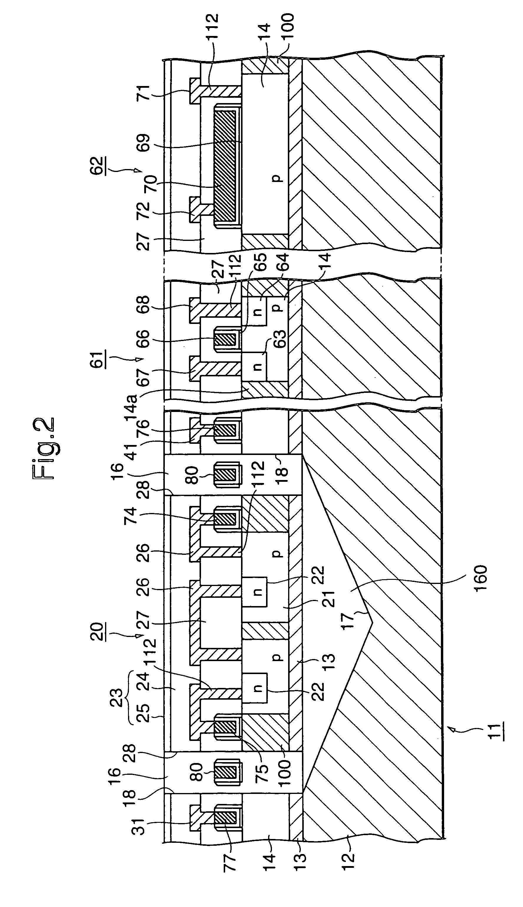
[0060] In the drawings, a semiconductor substrate 11 is composed of a single crystalline silicon semiconductor supporting substrate 12, an embedded silicon oxide insulating layer 13 provided on the substrate 12 and a single crystalline silicon semiconductor layer (SOI) layer 14. Such a substrate construction is called a silicon-on-insulator (SOI) construction.

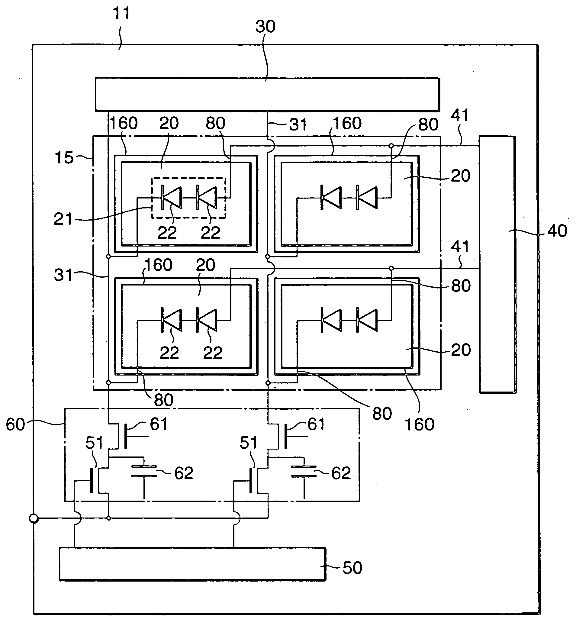
[0061] Partitioned on the substrate 11 is an infrared detection region 15, within which multiple holes 16 and cavities 160 are arranged in a lattice. Each cavity 160 is reversed pyramid in shape and the hole 16 is open on the side of the SOI layer 14 of the substrate 11, thus penetrating the SOI layer 14 and the insulating layer 13 down to the semiconductor supporting substrate 12 and having its bottom surface the supporting substrate.

[0062] Infrared detection pixels 20 are disposed within the cavity 160 to be arranged into a matrix of two...

second embodiment

[0131] An infrared detection sensor according to the present invention will then be discussed.

[0132] FIGS. 8(a), (b) and (c) illustrate an infrared detection pixel portion according to a second embodiment of the present invention, wherein like reference characters denote like parts as in the first embodiment.

[0133] As shown in FIG. 8(b) illustrating an enlarged cross section of a supporting beam line 80a in relation to the first embodiment shown in FIG. 2, the construction is of Step (i) in FIG. 7, a construction of a supporting beam line 80 from which a damascene metal 108 has been eliminated.

[0134] In addition, it is shown on the surface layout of FIG. 8(a) that the supporting beam line 80a is linearly formed and considerably lessened in length.

[0135] Specifically, in this embodiment, because of the elimination of the damascene metal 108 which predominates the heat conduction through the supporting beam line 80a, the thermal conductivity per unit length of the supporting beam l...

fourth embodiment

[0152] As a result, the supporting beam line 80c serving also as a supporting leg as shown in the fourth embodiment can be implemented linearly, thereby considerably improving a fill factor, the ratio of the area of the infrared detection portion 20 occupied by the pixel. The aforementioned effect of optical sensitization may thereby be obtained as well.

[0153] In addition, since the supporting beam line according to the fourth embodiment has a linear pattern, its mechanical strength and stability will considerably be improved as well analogously to the first and second embodiments.

[0154] Conversely, if the supporting beam line according to this embodiment were applied to the supporting structure which has a spiral pattern, then its sensitivity would approximately be fifty times as high.

[0155] It is of course possible also in this case to leave the STI region 100 at the bottom of the supporting beam line 80c as shown in FIG. 7(g), with an increased heat conduction. Considering the ...


PUM


Abstract

A supporting beam line for supporting, afloat in a cavity on a semiconductor substrate, an infrared detection pixel comprising an infrared absorption portion for absorbing an incident infrared ray and converting it into heat and a thermoelectric conversion portion for converting a temperature change caused by the heat generated in the infrared absorption portion into an electric signal is formed by a damascene metal on the same layer as the gate of a damascene metal gate MOS transistor to be used in a peripheral circuit. The supporting beam line comprises a conductor line with U-shaped cross section inside which a metal is filled.

Description

CROSS-REFERENCE TO RELATED APPLICATIONS [0001] This application is based upon and claims the benefits of priority from the prior Japanese Patent Application No. 2001-100402 filed on Mar. 30, 2001; the entire contents of which are incorporated herein by reference. BACKGROUND OF THE INVENTION [0002] 1. Field of the Invention [0003] The present invention relates to an infrared sensor and a manufacturing method thereof and, in particular, to a pixel construction of an uncooled infrared sensor and a manufacturing method thereof. [0004] 2. Related Art [0005] Infrared image sensing is characterized in its ability to pick up images at night as well as during the daytime and its higher transmittance to smoke and fog than visible radiation. Being capable of acquiring temperature information of an object to be sensed, infrared image sensors are adaptable to a variety of applications, such as a monitor camera and a fire detection camera, besides the field of defense. [0006] In recent years, ext...

Claims


Application Information

Patent Timeline
IPC IPC(8): G01J5/20G01J1/02G01J5/24H01L21/28H01L27/14H01L27/146H01L27/16H01L29/423H01L29/43H01L29/49H01L29/786H01L31/09H01L37/02
CPCG01J5/08G01J5/0853H01L27/16H01L27/14649G01J5/20H10N19/00H01L31/09H01L27/14G01J1/02
Inventor IIDA, YOSHINORISHIGENAKA, KEITAROMASHIO, NAOYA
Owner KK TOSHIBA
Why Eureka
Try Eureka