High density methods for producing diode-pumped micro lasers

a diode-pumped, micro-laser technology, applied in semiconductor lasers, biochemistry apparatus and processes, active medium materials, etc., can solve the problems of low beam quality, high cost, and inability to produce green wavelengths with substantial output power, etc., to achieve high beam quality, high beam quality, and high beam quality. high-density

Inactive Publication Date: 2005-03-24
SNAKE CREEK LASERS
View PDF19 Cites 76 Cited by
  • Summary
  • Abstract
  • Description
  • Claims
  • Application Information

AI Technical Summary

Benefits of technology

[0015] This invention addresses methods for producing high-density low-cost micro and miniature laser resonators capable of providing high beam quality laser radiation that can be assembled in highly compact packages using fabrication methodologies compatible with mass production and low unit costs (<$100.). The techniques and methods described in this disclosure thus provide solutions to the challenge of designing for manufacturability using mass production techniques characterized by their simplicity, cost effectiveness and adaptablity to operation at many different modes and a variety of wavelengths in either the visible or beyond. The invention further emphasizes those packaging technologies, fabrication processes, laser designs and materials that can provide high performance without compromising reliability of the microlaser devices, all with per unit materials' cost that can be as low as less than a few $100's even for more complex microchips. This makes the miniature devices produced according to the principles of the invention suitable to be integrated into numerous applications including those in the consumer and biomedical markets, potentially supplanting and replacing existing diode laser technology. The techniques disclosed also lend themselves to microlasers that can produce radiation at a large variety of operational modes and wavelengths. Specifically, the present invention provides improved methods, systems, and devices for providing cost effectively operational modes that include SLM in both CW and pulsed versions and spectral ranges that extend into the eyesafe regime on one end and the UV on the other.

Problems solved by technology

While diode lasers can provide wavelength coverage in the blue, red, and near infrared regions, currently no diode laser technology can produce green wavelengths with any substantial output power.
In addition, diode lasers are typically low-brightness devices with an astigmatic output due to the disparity in divergence angles in the directions parallel and perpendicular to the diode stripe.
On the other hand, solid state lasers—even compact modern diode-pumped, versions—tend to be too bulky and / or expensive to be used in mass applications such as supermarket scanners or for writing compact disks.
However, these means all tend to add bulk and cost to the systems, even when simple diode pumped designs are utilized.
There are known limitations to any extracavity nonlinear process that tend to limit the efficiency of harmonic conversion—especially where high peak powers are not available, as in the case of, e.g., CW lasers where SHG efficiencies are generally less than 5%.
This type of laser assembly is however labor-intensive to produce and relatively expensive.
Whereas Mooradian taught the use of transparent optical cement to bond laser and nonlinear materials, the bonding techniques of the monolithic structures did not allow for joining coated surfaces and the stringent requirements placed on cavity lengths produced lasers that were susceptible to mode hopping noise and were, in practice, difficult to fabricate efficiently with the desired quantities, production economies and costs.
Such an approach may again require more sophisticated fabrication techniques that may require separate processing for each microchip composite, making the process more difficult to apply to a mass production environment.
This configuration is often referred to as a flat-flat resonator, and in the sense understood by laser designers, is unstable.
While optically robust, the method of contact bonding individual crystals is, however, still rather expensive, with cost and yield issues.
The remaining portion of expensive crystal material is thus wasted making it difficult to further minimize the materials cost of each completed assembly.
Further cost reductions with this prior art technique are made difficult by the fact that is not practicable to make contact-bonded crystal assemblies much smaller because of difficulties associated with contacting small area surfaces together.
With current fabrication technologies, it is therefore difficult to reduce the unit cost, which tends to exceed $1000.00 per unit.
Such semiconductor based devices tend, however, to have relatively high costs of production, requiring major investment in processing facilities and are limited in their output wavelengths to those that can be efficiently produced by semiconductor quantum well structures.
Thus, visible lasers based on the VCSEL architecture are generally still too bulky and costly to meet the needs of mass applications such as pointers, supermarket scanners and construction aids, which rely at present on diode lasers priced at less than $100 a unit.
Mechanical adjustments can however, result, in stresses to the optical components, compromising alignment and output stability properties, especially if nonlinear elements are to be included in the cavity.

Method used


Image

  • High density methods for producing diode-pumped micro lasers
  • High density methods for producing diode-pumped micro lasers
  • High density methods for producing diode-pumped micro lasers

Examples


Embodiment Construction

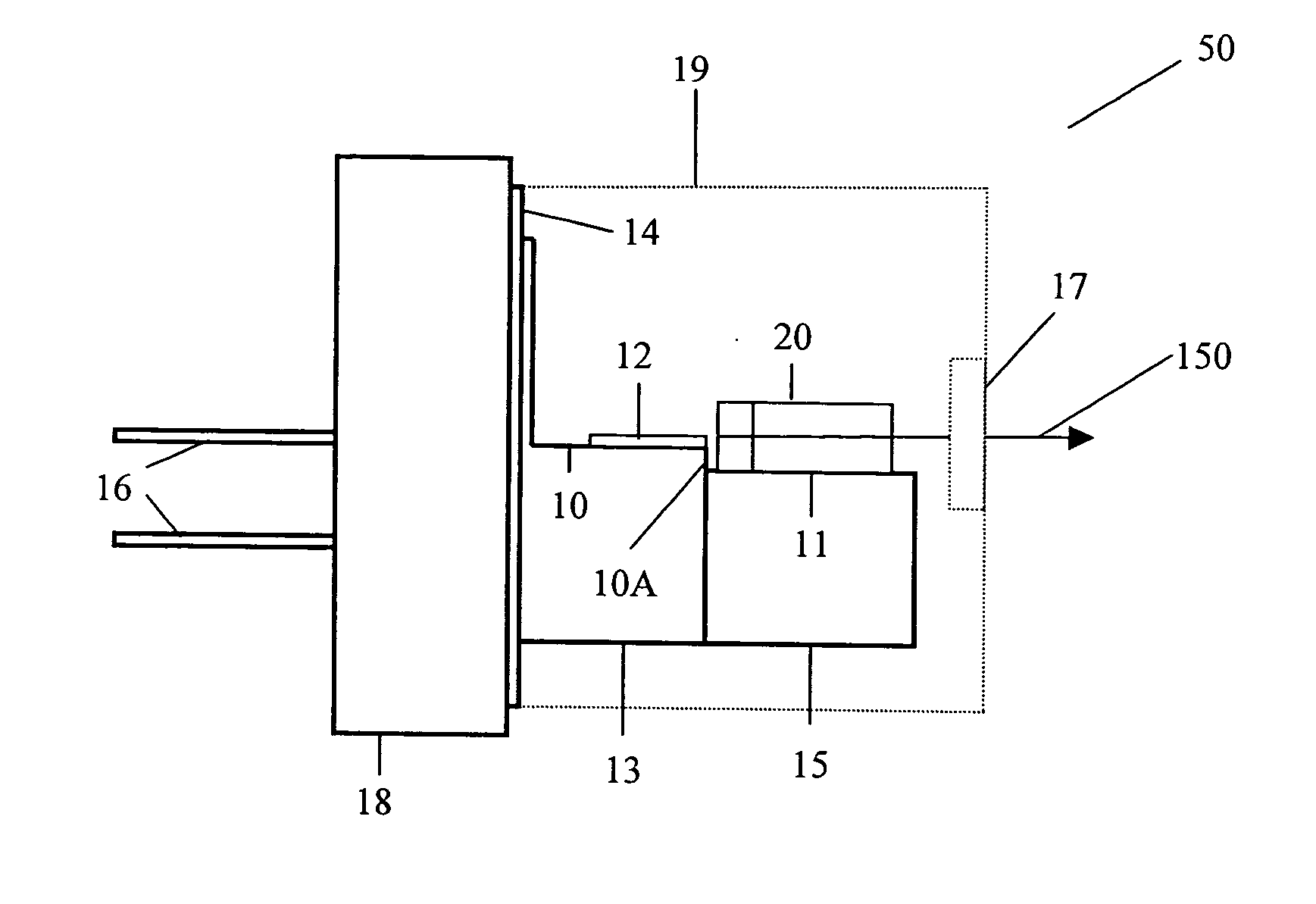
[0036] In order to construct miniature high-density low cost lasers three key design and processing aspects must be addressed. These are packaging, crystal fabrication and resonator design. The present invention incorporates unique features in each of these areas that allow various combinations of materials and components to be fabricated so as to address a wide range of operational modalities, but all sharing the common feature of compatibility with miniaturized, low cost, mass producible devices. Turning our attention to the three key design aspects these are discussed separately next.

[0037] 1. Packaging:

[0038] In order to package microchips into useful and mass-producible devices it is important to have a package, that will serve to minimize the overall laser volume while providing the functionality required for laser operation and the low costs associated with mass applications. In one preferred embodiment, a standard diode TO (transistor outline) package is modified to accomm...


PUM

PropertyMeasurementUnit
poweraaaaaaaaaa
poweraaaaaaaaaa
green power outputaaaaaaaaaa

Abstract

A miniaturized laser package is provided comprising a standard semiconductor laser package modified to accept a solid state microchip assembly pumped by the diode laser. Standard packages described in the invention include TO and HHL packages all of which are characterized by small dimensions, well sealed housing, robust mounting features, known characterized materials and economical production and assembly techniques characteristic of the semiconductor processing industry. In particular, the microchip lasers are produced using high density techniques that lend themselves to mass production, resulting in very low unit costs. At the same time, the compact laser devices provide a solution to the problem of providing laser radiation at high beam quality and good reliability features with a variety of wavelengths and operational characteristics and low noise features not available from diode lasers yet relying primarily on standardized designs, materials and techniques common to diode laser manufacturing. The devices constructed according to methods taught by the invention can therefore be readily integrated into numerous applications where power, reliability and performance are at a premium but low cost is essential, eventually replacing diode lasers in many existing systems but also enabling many new commercial, biomedical, scientific and military systems.

Description

[0001] This application claims the benefit of priority from Provisional U.S. Patent Application Ser. No. 60 / 504,617 filed Sep. 22, 2003.FIELD OF THE INVENTION [0002] The present invention relates to highly compact and / or miniaturized diode pumped solid state lasers that are manufacturable using mass production techniques. BACKGROUND OF THE INVENTION [0003] New types of microlasers are desired as a replacement for conventional red lasers, particularly red semiconductor diode lasers that are commonplace in many applications including pointing devices, supermarket scanners, gun pointers, and others. While diode lasers can provide wavelength coverage in the blue, red, and near infrared regions, currently no diode laser technology can produce green wavelengths with any substantial output power. Yet, the green wavelength region is particularly important because it is the region where the spectral responsivity of the human eye is a maximum and where underwater transmission peaks. In additi...

Claims


Application Information

Patent Timeline
Patent Type & Authority Applications(United States)
IPC IPC(8): C12QH01S3/02H01S3/04H01S3/042H01S3/06H01S3/07H01S3/091H01S3/0941H01S3/108H01S3/109H01S3/113H01S3/131H01S3/16H01S5/00
CPCH01S3/025H01S3/0405H01S3/042H01S3/0604H01S3/0627H01S3/1673H01S3/108H01S3/109H01S3/113H01S3/1317H01S3/1611H01S3/09415H01S3/091
Inventor BROWN, DAVID C.
Owner SNAKE CREEK LASERS
Why Eureka
Try Eureka