Method of plating a metal or metal or metal compound on a semiconductor substrate that includes using the same main component in both plating and etching solutions

a technology of metal or metal compound and semiconductor substrate, which is applied in the direction of semiconductor devices, metallic material coating processes, electrical equipment, etc., can solve the problems of affecting the semiconductor element formed on the semiconductor substrate, affecting the performance of transistors, and deviation of wiring patterns, so as to reduce the roughness of the surface of copper film, reduce the difficulty of etching, and the effect of fewer steps

a technology of metal or metal compound and semiconductor substrate, which is applied in the direction of semiconductor devices, metallic material coating processes, electrical equipment, etc., can solve the problems of affecting the semiconductor element formed on the semiconductor substrate, affecting the performance of transistors, and deviation of wiring patterns, so as to reduce the roughness of the surface of copper film, reduce the difficulty of etching, and the effect of fewer steps

US20050064700A1Inactive Publication Date: 2005-03-24KK TOSHIBA

Image

  • Method of plating a metal or metal or metal compound on a semiconductor substrate that includes using the same main component in both plating and etching solutions
  • Method of plating a metal or metal or metal compound on a semiconductor substrate that includes using the same main component in both plating and etching solutions
  • Method of plating a metal or metal or metal compound on a semiconductor substrate that includes using the same main component in both plating and etching solutions

Examples


Embodiment Construction

[0050] Preferred embodiments of the present invention will now be described with reference to the accompanying drawings.

[0051] This invention is adapted to, for example, a pillar process, a single damascene structure and a dual damascene structure in a multilayer wiring structure of a semiconductor device.

[0052] (1) Pillar Process

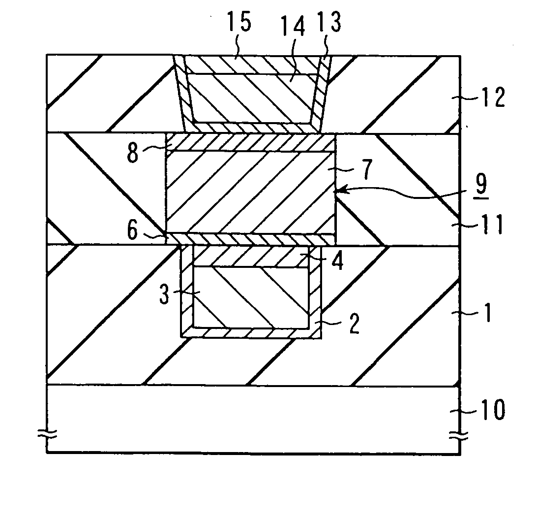
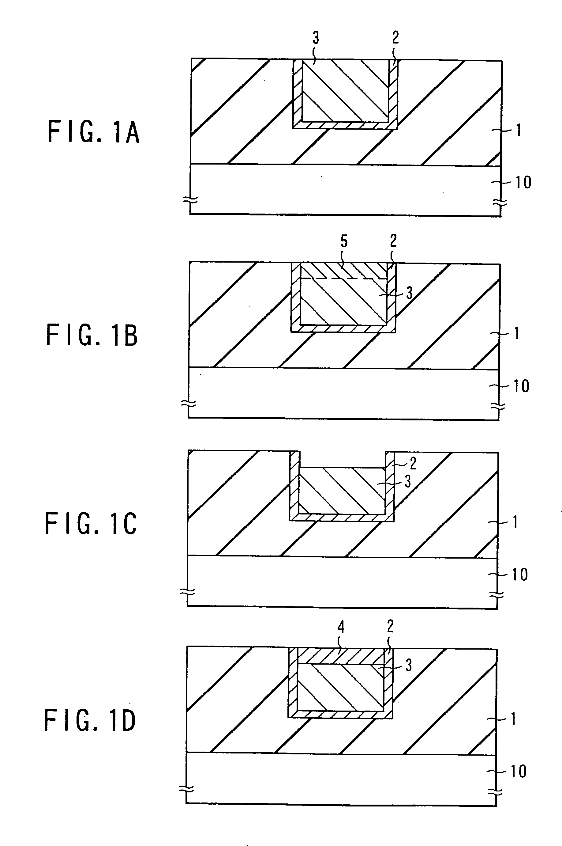
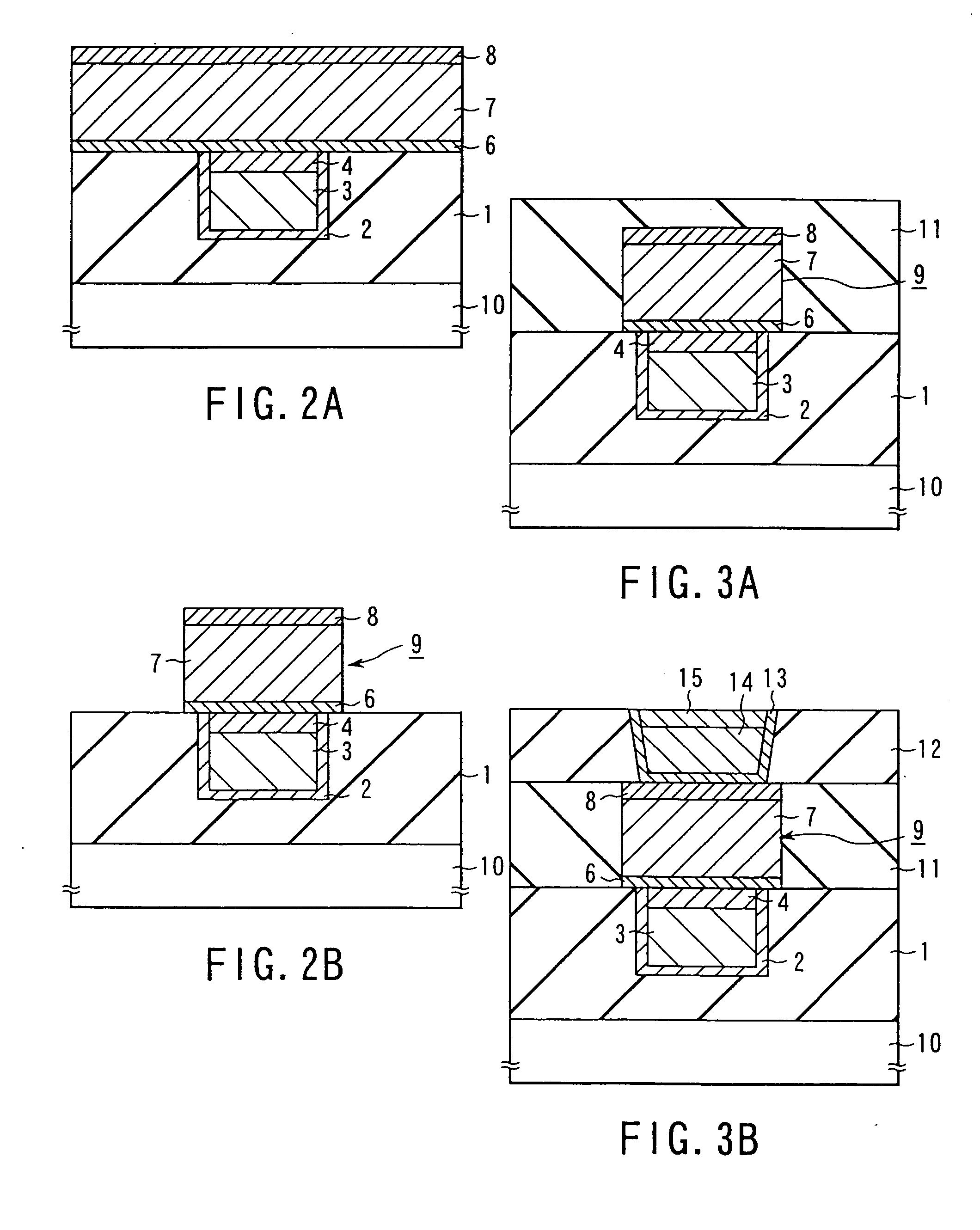
[0053]FIGS. 1A through 1D are cross-sectional views of a semiconductor substrate on which multilayer wirings are formed. A pillar wiring (contact wiring) which is formed by this process connects an under-lying wiring to an over-lying wiring. As shown in FIGS. 1A to 1D, the under-lying wiring is buried in an inter-layer insulating film 1. The inter-layer insulating film 1 is formed of silicon oxide on a semiconductor substrate 10 of silicon or the like where a semiconductor element (not shown) such as an integrated circuit is formed, and wiring grooves are formed in the surface of this inter-layer insulating film 1. A barrier metal layer 2 of a conductive...


PUM

PropertyMeasurementUnit
Concentrationaaaaaaaaaa
Semiconductor propertiesaaaaaaaaaa

Abstract

A method of forming a copper oxide film including forming a copper oxide film including an ammonia complex by causing a mixed solution of aqueous ammonia and aqueous hydrogen peroxide, which has been adjusted to have pH of 8 to 10 or pH of 9 to 10, to contact a surface of a copper film. A method of fabricating a semiconductor device including burying a copper film to be a wiring or a contact wiring in a wiring groove or a contact hole formed in a surface of an insulating film formed on a semiconductor substrate, or in both the wiring groove and the contact hole, forming a copper oxide film including an ammonia complex on a surface of the copper film by using the copper oxide film forming method, and removing the copper oxide film from the copper film using acid or alkali.

Description

CROSS-REFERENCE TO RELATED APPLICATION [0001] This application is based upon and claims the benefit of priority from the prior Japanese Patent Application No. 2000-015653, filed Jan. 25, 2000; the entire contents of which are incorporated herein by reference. BACKGROUND OF THE INVENTION [0002] The present invention relates to a semiconductor device such as a semiconductor integrated circuit, a method of processing a copper film to be used for wirings for a semiconductor device such as a semiconductor integrated circuit and a method of producing a wiring structure for such a semiconductor device. [0003] Today, copper or a material essentially consisting of copper is used for wirings for a semiconductor device such as a semiconductor integrated circuit. In such a case, copper atoms are diffused into an insulating film to enter the semiconductor substrate, which may result in malfunction of transistors. To prevent it, a barrier metal layer of a titanium nitride, tantalum nitride, tungs...

Claims


Application Information

Patent Timeline
24 Mar 2005
Publication
US20050064700A1
IPC
C23C22/63; H01L21/308; H01L21/28; H01L21/288; H01L21/3205; H01L21/768
CPC
C23C22/63; H01L21/02074; H01L21/02087; H01L21/0209; H01L21/3212; H01L21/76888; H01L21/76849; H01L21/76865
Inventors
UOZUMI, YOSHIHIRO