Organic electroluminescent device

Active Publication Date: 2005-04-21
MITSUBISHI HEAVY IND LTD +1
View PDF39 Cites 239 Cited by
  • Summary
  • Abstract
  • Description
  • Claims
  • Application Information

AI Technical Summary

Benefits of technology

[0028] The present invention is also devised in view of these circumstances, and thus the present invention disposes, adjacent to the anode electrode layer, a hole injection layer having a novel structure

Problems solved by technology

However, since magnesium is liable to be oxidized and instable and also has poor adhesion to the surface of the organic material, Tang et al. have suggested to use magnesium alloyed with silver (Ag: work function of 4.6 eV), since silver is relatively stable, and thus has a high work function and good adhesion to the surface of the organic material.
Furthermore, in the Kodak patents described above, it is disclosed that the alkaline metals having the lowest work function, should be removed from the candidate examples of the cathode metal, even though they can exhibit excellent function in principle, because they have an excessively high reactivity for achieving the stable driving of the EL devices.
On the other hand, generally, many of the Lewis acid compounds are chemic

Method used


Image

  • Organic electroluminescent device
  • Organic electroluminescent device
  • Organic electroluminescent device

Examples


example 1

[0087] In this example, the organic EL device having the lamination structure of FIG. 5 is fabricated.

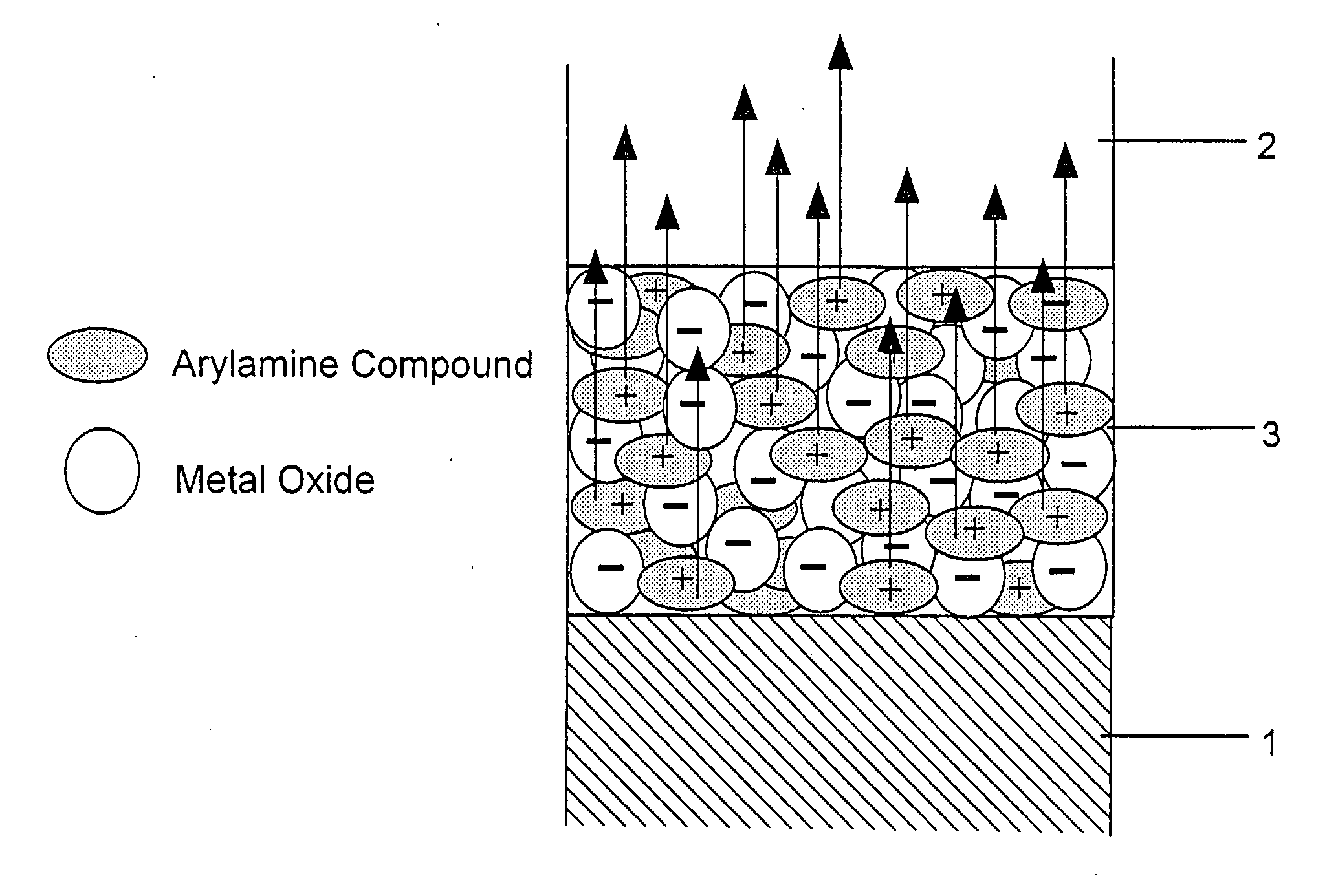
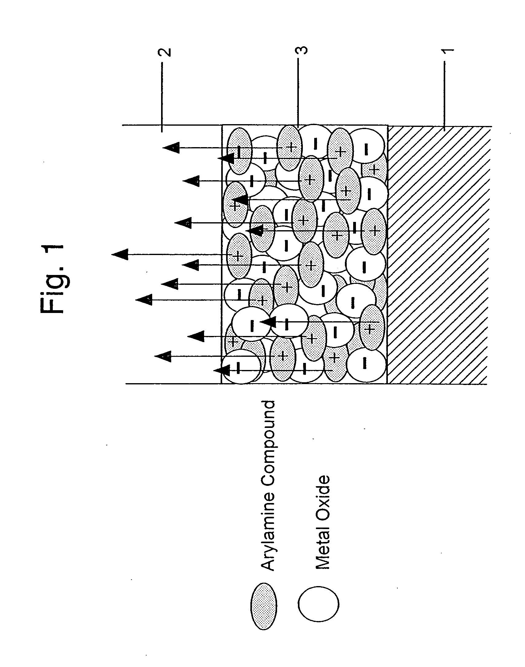
[0088] A glass substrate 21 is coated thereon with an ITO (indium-tin oxide; Nippon Sheet Glass Co., Ltd.) having a sheet resistance of about 10 Ω / □ as a transparent anode electrode layer (anode electrode layer) 22. A metal oxide, V2O5, and an organic compound having a hole transporting property, α-NPD, are co-deposited at a molar ratio of V2O5: α-NPD of about 4:1 on the ITO-coated glass substrate 21 to form a mixed layer 27 having a thickness of about 100 Å acting as a hole injection layer.

[0089] Thereafter, a hole transportation layer (α-NPD) 23, a light-emissive layer (Alq) 24, an electron injection layer (metal doping layer, low resistance electron transportation layer) 25 and a cathode electrode layer (cathode) 26 are sequentially laminated as in the production of the EL device of the above-described Reference Example. Note that an organic structure 28 including a light-emiss...

example 2

[0091] In this example, the organic EL device having the lamination structure of FIG. 6 is fabricated.

[0092] A glass substrate 31 is coated thereon with an ITO (indium-tin oxide; Nippon Sheet Glass Co., Ltd.) having a sheet resistance of about 10 Ω / □ as a transparent anode electrode layer 32. A metal oxide, V2O5, and an organic compound having a hole transporting property, α-NPD, are co-deposited at a molar ratio of about 4:1 on the ITO-coated glass substrate 31 to form a mixed layer 37 having a thickness of about 1,000 Å acting as a hole injection layer of the present invention.

[0093] Thereafter, a hole transportation layer (α-NPD) 33, a light-emissive layer (Alq) 34, an electron injection layer (metal doping layer) 35 and a cathode electrode layer 36 are sequentially laminated as in the fabrication of the EL device of the above-described Reference Example. Note that an organic structure 38 including a light-emissive layer is formed from the hole transportation layer 33, the ligh...

example 3

[0099] In this example, the organic EL device having the top emission structure of FIG. 12 is fabricated. An aluminum (Al; work function of about 4.2 eV) is deposited at the deposition rate of about 10 Å / sec under the pressure of about 10−6 Torr (1 Torr=133.32 Pa) (hereinafter, all deposition process is conducted under the same condition) on a glass substrate 41 to form an anode electrode layer 42 having a thickness of about 1,000 Å. A metal oxide, V2O5, and an organic compound having a hole transporting property, α-NPD, are co-deposited at a molar ratio of about 4:1 on an anode electrode layer 42 to form a mixed layer 47 having a thickness of about 100 Å acting as a hole injection layer of the present invention. Thereafter, α-NPD is deposited at the deposition rate of about 2 Å / sec on the hole injection layer 47 to form a hole transporting layer 43 having a thickness of about 600 Å. Subsequently, Alq is deposited on the hole transportation layer 43 under the same vapor deposition c...


PUM

PropertyMeasurementUnit
Glass transition temperatureaaaaaaaaaa
Electrical resistivityaaaaaaaaaa

Abstract

An organic electroluminescent device includes an anode electrode layer; a cathode electrode layer opposed to the anode electrode layer; a hole injection layer provided adjacent to the anode electrode layer an organic structure including at least one light-emissive layer_or at least one light-emissive unit having at least one light-emissive layer; between the anode electrode layer and the cathode electrode layer. At least one of the anode electrode layer and the cathode electrode layer is transparent. The hole injection layer includes a mixed layer of a metal oxide and an organic compound. The mixed layer is formed upon co-deposition of the metal oxide and the organic compound.

Description

CROSS REFERENCE TO RELATED APPLICATION [0001] The present application is related to and claims priority of the following co-pending application, namely, Japanese patent application number 2003-358402 filed on Oct. 17, 2003. BACKGROUND OF THE INVENTION [0002] 1. Field of the Invention [0003] The present invention relates to an organic electroluminescent device (hereinafter, abbreviated as an “organic EL device”) which can be used as a planar light source or as a display device. [0004] 2. Description of the Related Art [0005] Attention has been made to an organic electroluminescent device in which a light-emissive layer is constituted from an organic compound, because such a device can ensure a large area display at a low driving voltage. To highly increase the efficiency of organic EL devices, Tang et al. of Eastman Kodak Company, as is disclosed in Appl. Phys. Lett., 51, 913 (1987), have successfully achieved an EL device which can exhibit a high luminance and sufficient efficiency ...

Claims


Application Information

Patent Timeline
IPC IPC(8): C09K11/06H01L51/00H01L51/30H01L51/50H05B33/14
CPCH01L51/0052H01L51/0059H01L51/5088H01L51/0077H01L51/0081H01L51/0062H10K85/649H10K85/615H10K85/631H10K85/30H10K85/324H10K50/17C09K11/06H05B33/14
Inventor KIDO, JUNJIMATSUMOTO, TOSHIONAKADA, TAKESHIKAWAMURA, NORIFUMI
Owner MITSUBISHI HEAVY IND LTD
Why Eureka
Try Eureka