Photoresist polymer and photoresist composition containing the same

a technology of photoresist polymer and composition, applied in the field of photoresist polymer and photoresist composition, can solve the problems of difficult to improve the ler of the pattern, improper use at 157 nm wavelength, and more severe ler when using arf photoresist materials, etc., to achieve excellent transmittance, low light absorption, and thermal resistance and adhesive properties. good

Inactive Publication Date: 2005-04-28
SK HYNIX INC
View PDF20 Cites 14 Cited by
  • Summary
  • Abstract
  • Description
  • Claims
  • Application Information

AI Technical Summary

Benefits of technology

[0010] Disclosed herein are photoresist polymers that have excellent transmittance, etching resistance, thermal resistance and adhesive property, low light absorbance and high affinity to an developing solution, thereby obtaining patterns with improved LER.

Problems solved by technology

However, since the thickness of photoresist materials becomes thinner as circuits of semiconductor devices become more microfine, it is difficult to improve the LER of the patterns.
Conventional photoresist materials have also strong light absorbance at a wavelength of 157 nm, thus they are improper for use at 157 nm wavelength.
As a result, since the ArF photoresist materials have low affinity to basic development solutions, the LER occurs more severely when using ArF photoresist materials.
However, such polyethylene and polyacrylate resins comprising fluorine have low etching resistance and decreased adhesive properties to a silicon substrate.
Furthermore, the polyethylene and polyacrylate resins are not suitable to be used commercially because they are expensive and their mass-production is difficult.
Moreover, the protecting group of the conventional photoresist polymer is destroyed in the baking process after exposure and generates gases when patterns are formed using chemically-amplified photoresists, resulting in the damage of the lens.
This phenomenon occurs inevitably when patterns are formed using chemically amplified photoresists, and decreased stability of the subsequent processes results in the reduction of the yield of the semiconductor devices.

Method used

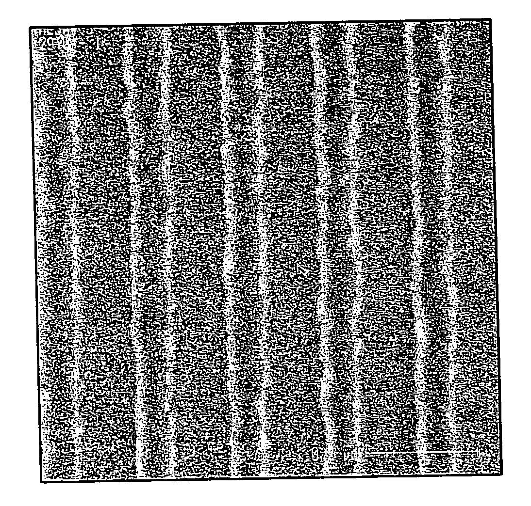
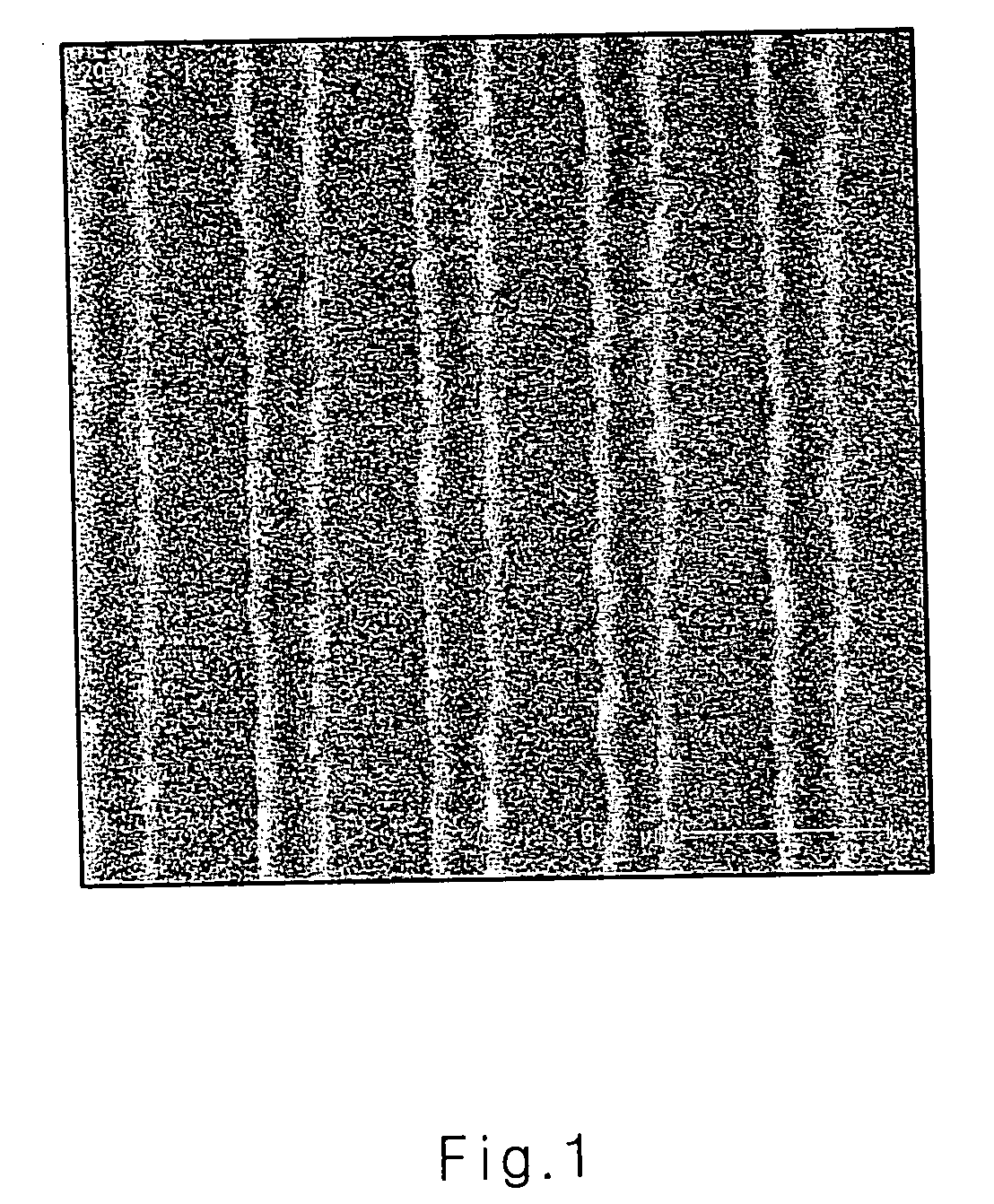
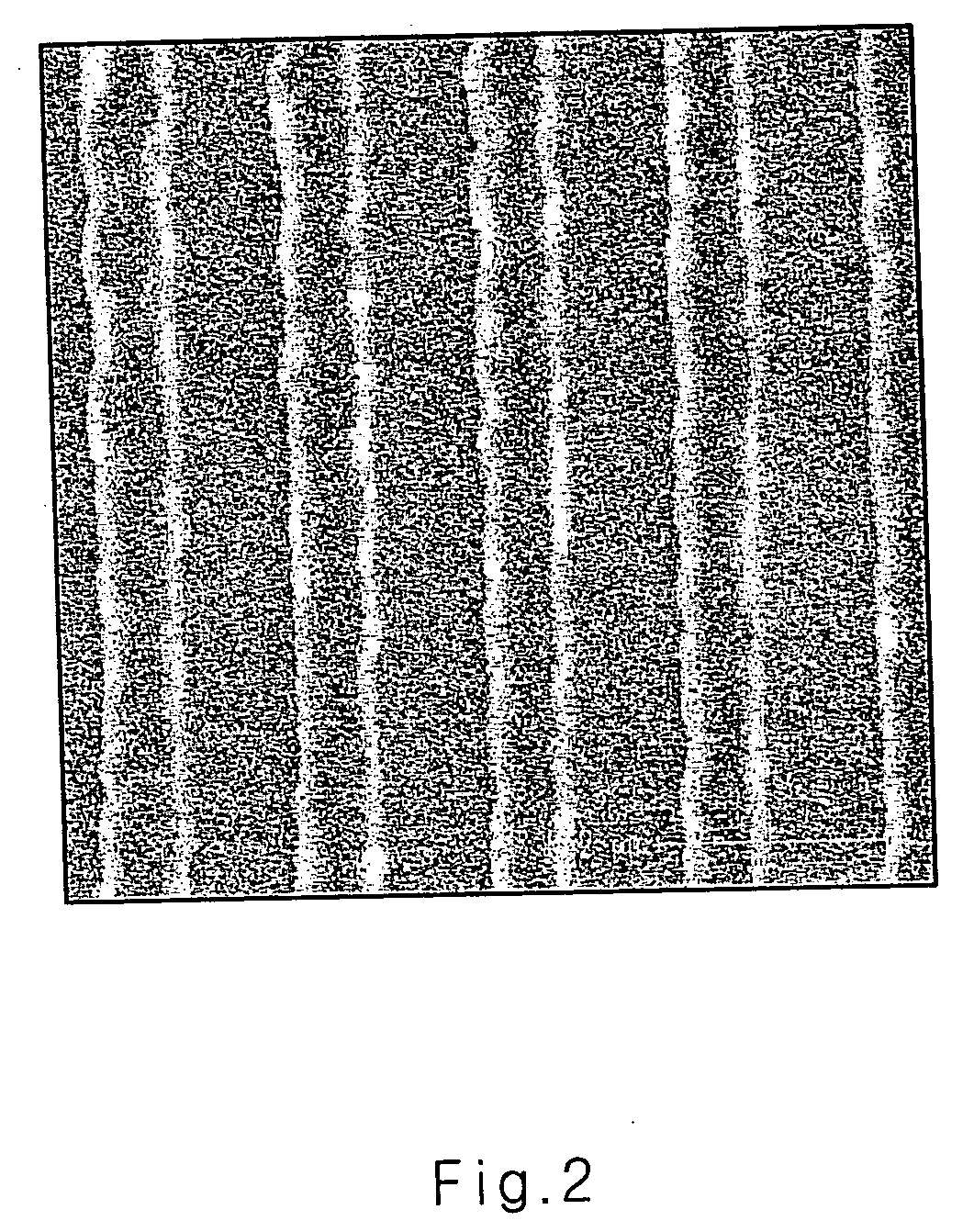

Image

  • Photoresist polymer and photoresist composition containing the same
  • Photoresist polymer and photoresist composition containing the same
  • Photoresist polymer and photoresist composition containing the same

Examples


example 1

Synthesis of Compound of Formula 1b

[0107] 0.1M of 2,3,3-trimethyl-1,3-propane sultone was dissolved in tetrahydrofuran anhydride under a nitrogen atmosphere, and 0.1M of NaH was added thereto. The prepared solution was stirred for 10 minutes, and then 0.11M of vinyl bromide was added thereto. The obtained mixture was further reacted at room temperature for 3 hours. After the reaction was completed, the reacted mixture was filtered to remove NaBr. Then, by precipitation of the resulting material in a diethylether / pentane mixed solution, the compound of Formula 1b was obtained (yield: 92%).

example 2

Synthesis of Compound of Formula1c

[0108] The same procedure of Example 1 was performed using 2,2,3,3-tetramethyl-1,3-propane sultone instead of 2,3,3-trimethyl-1,3-propane sultone, and obtained the compound of Formula1c (yield: 96%).

example 3

Synthesis of Compound of Formula 1e

[0109] The same procedure of Example 1 was performed using 1,2,3,3-tetramethyl-1,3-propane sultone instead of 2,3,3-trimethyl-1,3-propane sultone, and obtained the compound of Formula 1e (yield: 92%).


PUM

PropertyMeasurementUnit
roughnessaaaaaaaaaa
roughnessaaaaaaaaaa
wavelengthsaaaaaaaaaa

Abstract

The present invention relates to photoresist polymers and photoresist compositions. The disclosed photoresist polymers and photoresist compositions containing the same have excellent transmittance, etching resistance, thermal resistance and adhesive property, low light absorbance and high affinity to a developing solution at a wavelength of 193 nm and 157 nm, thereby improving LER (line edge roughness).

Description

BACKGROUND [0001] 1. Technical Field [0002] The present invention relates to photoresist polymers and photoresist compositions comprising the same. More specifically, it relates to compounds represented by Formula 1 described herein as photoresist monomers, photoresist polymers containing the same, and photoresist compositions that have excellent transmittance, etching resistance, thermal resistance, adhesive property, and low light absorbance at a wavelength of 13 nanomometers (nm) as well as 193 nm and 157 nm and high affinity to a developing solution, thereby improving line edge roughness (hereinafter, referred to as “LER”). [0003] 2. Description of the Related Art [0004] In order to be used as photoresists for ArF and VUV (vacuum ultraviolet), photoresist polymers and photoresist compositions are required to have low light absorbance at wavelengths of 193 nm and 157 nm, excellent etching resistance and adhesive property on the substrate, and to be developed with 2.38 wt % and 2....

Claims


Application Information

Patent Timeline
Patent Type & Authority Applications(United States)
IPC IPC(8): C07D327/04C08F28/06G03C1/76G03F7/004G03F7/039G03F7/20H01L21/00H01L21/027
CPCC07D327/04G03F7/0397G03F7/0046
Inventor LEE, GEUN SU
Owner SK HYNIX INC
Why Eureka
Try Eureka