Semiconductor device and process of producing the same

a technology of semiconductor devices and resistors, which is applied in the direction of semiconductor devices, diodes, resistors, etc., can solve the problems of difficult to both control the resistance value to a desired value, provide a temperature dependence of resistance that is substantially zero, and provide resistors of desired resistance values. , to achieve the effect of convenient manufacturing

Inactive Publication Date: 2005-05-12
RENESAS ELECTRONICS CORP
View PDF37 Cites 19 Cited by
  • Summary
  • Abstract
  • Description
  • Claims
  • Application Information

AI Technical Summary

Benefits of technology

[0025] Accordingly, by the present invention a conducting structure, formed of polycrystalline silicon layers, can be provided, having a desired resistance value and a desired temperature dependence of resistance (including a temperature dependence of resistance that is substantially

Problems solved by technology

, and this poses a serious problem in designing circuits in a case where the resistors of that sort are employed in integrated circuits.
The foregoing disclosed structures have problems in providing resistors of desired resistance values and with no (or substantially no) temperature dependence of resistance over the temperature range of use of the resistor.
For example, where only a single layer or single region is used, it is difficult to both control the resistance value to a desired value, and to provide a temperature dependence of resistance that is substantially zero.
Moreover, fabrication difficulties arise, or the manufacturing is made more complex, by electrically connecting a semiconductor region in, e.g., a single-crystal silicon substrate to a polycrystalline silicon layer (either by forming the polycrystalline silicon directly on the semiconductor region or electrically connecting an overlying polycrystalline silicon layer to a region in a single-crystal silicon substrate).
However, the improvement of the temperature dependence with respect to any given specific resistance value cannot technically be provided, and this means different processes of manufacture will have to be adopted for different resistance values of different resistors, even where the different resistors are on a same substrate of a same semiconductor device.
Moreover, there arises a problem in that polycrystalline sil

Method used


Image

  • Semiconductor device and process of producing the same
  • Semiconductor device and process of producing the same
  • Semiconductor device and process of producing the same

Examples


embodiment 1

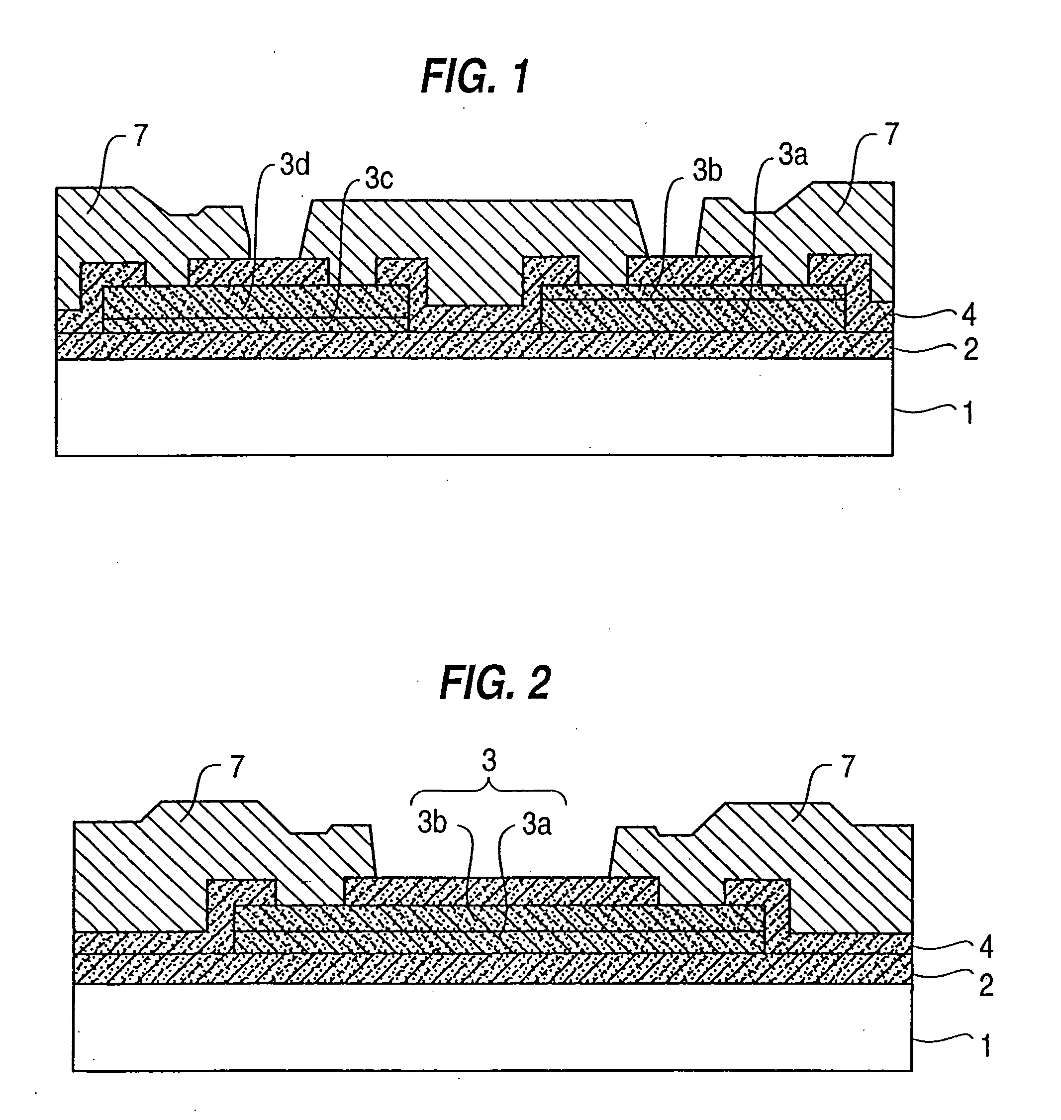
[0098] Referring to FIG. 2, a first embodiment of the present invention will be described. FIG. 2 illustrates a resistor embodying the present invention, wherein an attempt is made to improve temperature dependence of resistance (e.g., provide a resistor whose resistance is substantially independent of temperature over a temperature range of use of the resistor) by providing a polycrystalline silicon film 3 of two-layer structure including a first polycrystalline silicon layer 3a of small grain size and a second polycrystalline silicon layer 3b of large grain size. Thus, the resistor in FIG. 2 is constituted by the first and second polycrystalline silicon films 3a, 3b, the resistor being electrically connected at both ends to aluminum electrodes 7,7.

[0099] The prior art structure has shortcomings in that fluctuations in temperature dependence of resistance is dependent on resistivity, because polycrystalline silicon film or single crystal structure is used as a resistance material....

embodiment 2

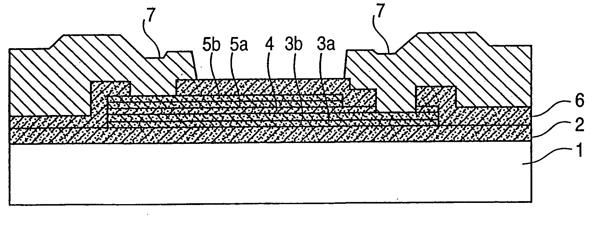
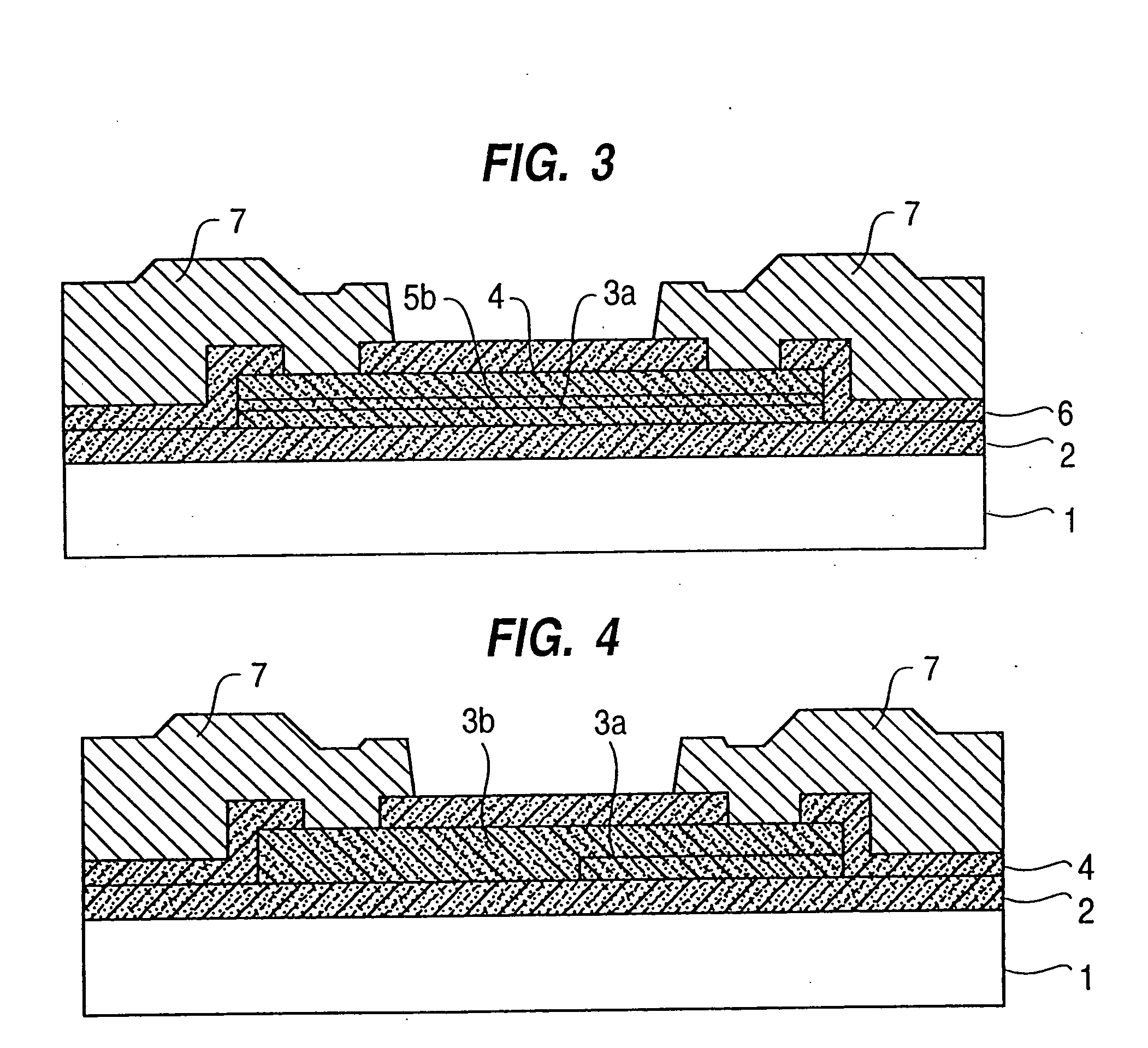
[0104] Referring to FIG. 3, a second embodiment will be described. FIG. 3 illustrates a resistor embodying the present invention, wherein an attempt is also made to improve temperature dependence of resistance by providing a polycrystalline silicon film of two-layer structure including a first polycrystalline silicon layer 3a of small grain size and a second polycrystalline silicon layer 5b of large grain size. More specifically, the two-layer structure of polycrystalline silicon is made attainable likewise by varying the deposition temperature at which the polycrystalline silicon of large grain size and that of small grain size are formed. However, the use of n-type impurities of such as phosphorous in that method may cause one or both of the polycrystalline silicon films to affect the other, or each other, as far as their crystal structure is concerned, during the process of crystallization with heat treatment, thus making it difficult to attain a two-layer structure of good quali...

embodiment 3

[0108] This embodiment 3 is an application of the improved temperature dependence resulting from the two-layer structure of polycrystalline silicon resistors shown in Embodiments 1 and 2.

[0109] As is clear from FIG. 1, two or more than two kinds of resistor layers 3a, 3b, 3c, 3d, different from each other in sheet resistance, are formed in polycrystalline silicon layers laid on one and the same substrate. If the methods referred to in Embodiments 1 and 2 are used (e.g., by carefully selecting the conditions of ion implantation when forming layers 3b and 3d), sheet resistance and temperature dependence may be varied as desired. In other words, the temperature dependence of two or more than two kinds of resistors different in sheet resistance can simultaneously be reduced to almost zero or slightly positive. Thus, each of the resistor formed by layers 3a and 3b, and the resistor formed by layers 3c and 3d, can have temperature dependence of resistance that is substantially zero (or w...


PUM


Abstract

The present invention provides a polycrystalline silicon conducting structure (e.g., a resistor) whose resistance value is controlled, and can be less variable and less dependent on temperature with respect to any resistant value, and a process of producing the same. Use is made of at least a two-layer structure including a first polycrystalline silicon layer of large crystal grain size and a second polycrystalline silicon layer of small crystal grain size, and the first polycrystalline silicon layer has a positive temperature dependence of resistance while the second polycrystalline silicon layer has a negative temperature dependence of resistance, or vice versa. Moreover, the polycrystalline silicon layer of large grain size can be formed by high dose ion implantation and annealing, or by depositing the layers by chemical vapor deposition at different temperatures so as to form large-grain and small-grain layers.

Description

BACKGROUND OF THE INVENTION [0001] The present invention relates to a semiconductor device using polycrystalline silicon resistors having only a small resistance value deviation, and whose resistance varies with a change in temperature at a desired level (including wherein the resistance value is substantially independent of a change in temperature), e.g., in the temperature range of use of the device. [0002] With respect to the prior art concerned with resistors using polycrystalline silicon, IEEE Transactions on Electron Devices, ED-28, No. 7 (1981), pp. 818-830, and Gray and Meyer, Analysis and Design of Analog Integrated Circuits, 2d Ed. (1984), John Wiley & Sons, Inc. disclose an arrangement of making one of the following a resistor, namely, (1) an impurity diffusion region in a semiconductor substrate, and (2) a polycrystalline silicon layer on a dielectric film. FIGS. 20-22 of the present application are sectional views of these structures, wherein numeral 1 denotes a silicon...

Claims


Application Information

Patent Timeline
IPC IPC(8): H01C7/06H01L21/02H01L21/822H01L27/04H01L27/06
CPCH01L27/0652H01L28/20H01L27/0688H01L27/04
Inventor SHIMAMOTO, HIROMIUCHINO, TAKASHISHIBA, TAKEOOHNISHI, KAZUHIROTAMAKI, YOICHIKOBAYASHI, TAKASHIKIKUCHI, TOSHIYUKIIKEDA, TAKAHIDE
Owner RENESAS ELECTRONICS CORP
Why Eureka
Try Eureka