Solar cell and process for producing solar cell

a technology of solar cells and solar cells, applied in the field of solar cells and processes for producing solar cells, can solve the problems of low conversion efficiency, increase in the number, and obstacles to overcome, so as to improve the photovoltaic conversion efficiency, avoid recombination, and reduce grain boundaries

Inactive Publication Date: 2005-05-19
MITSUBISHI HEAVY IND LTD
View PDF5 Cites 31 Cited by
  • Summary
  • Abstract
  • Description
  • Claims
  • Application Information

AI Technical Summary

Benefits of technology

[0012] The present invention was made in view of the above circumstances, and an object of the present invention is to provide a process for producing a solar cell which can enhance the photovoltaic conversion efficiency by enlarging the grain sizes in the direction of the thickness of an i-layer to reduce grain boundaries in the direction of the growth of grains, thereby avoiding recombination of carriers.
[0013] Another object of the present invention is to provide a process for producing a solar cell which can enhance the photovoltaic conversion efficiency by increasing the electric conductivities of an n-layer and a p-layer without changing the quality of an i-layer.
[0014] Yet another object of the present invention is to provide a solar cell in which electric conductivities of an n-layer and a p-layer are high and the sizes of grains in an i-layer are large in the direction the thickness of the i-layer, thereby possessing high photovoltaic conversion efficiency.

Problems solved by technology

However, there still remain obstacles to be overcome such as low conversion efficiency, in comparison with solar cells of bulk silicon types such as a single crystal or a polycrystal, and degradation.
Such obstacles are considered as disadvantages of amorphous silicon solar cells.
There has been a problem in that such increase in the number of microcrystalline grains results in increase in the number of grain boundaries which extend in the direction intersecting the direction of the thickness of the Si layers, and thus results in increase in the number of defects, which promote recombination of carriers, shortening the lifetime of the carriers, thereby making it difficult to improve cell performance.
On the other hand, a small number of crystal nucleation at the beginning of crystal growth and amorphous-rich condition at the beginning of formation of the i-layer also adversely affect cell performance.
However, even this two-stage film deposition method is not sufficient to reduce grain boundaries.
However, if thermal annealing for increasing the electric conductivity is carried out after forming PIN layers, a problem arises in some cases in that dopants in the n- and p-layers diffuse into the i-layer, resulting in reduction in photovoltaic conversion efficiency.

Method used


Image

  • Solar cell and process for producing solar cell
  • Solar cell and process for producing solar cell
  • Solar cell and process for producing solar cell

Examples


first embodiment

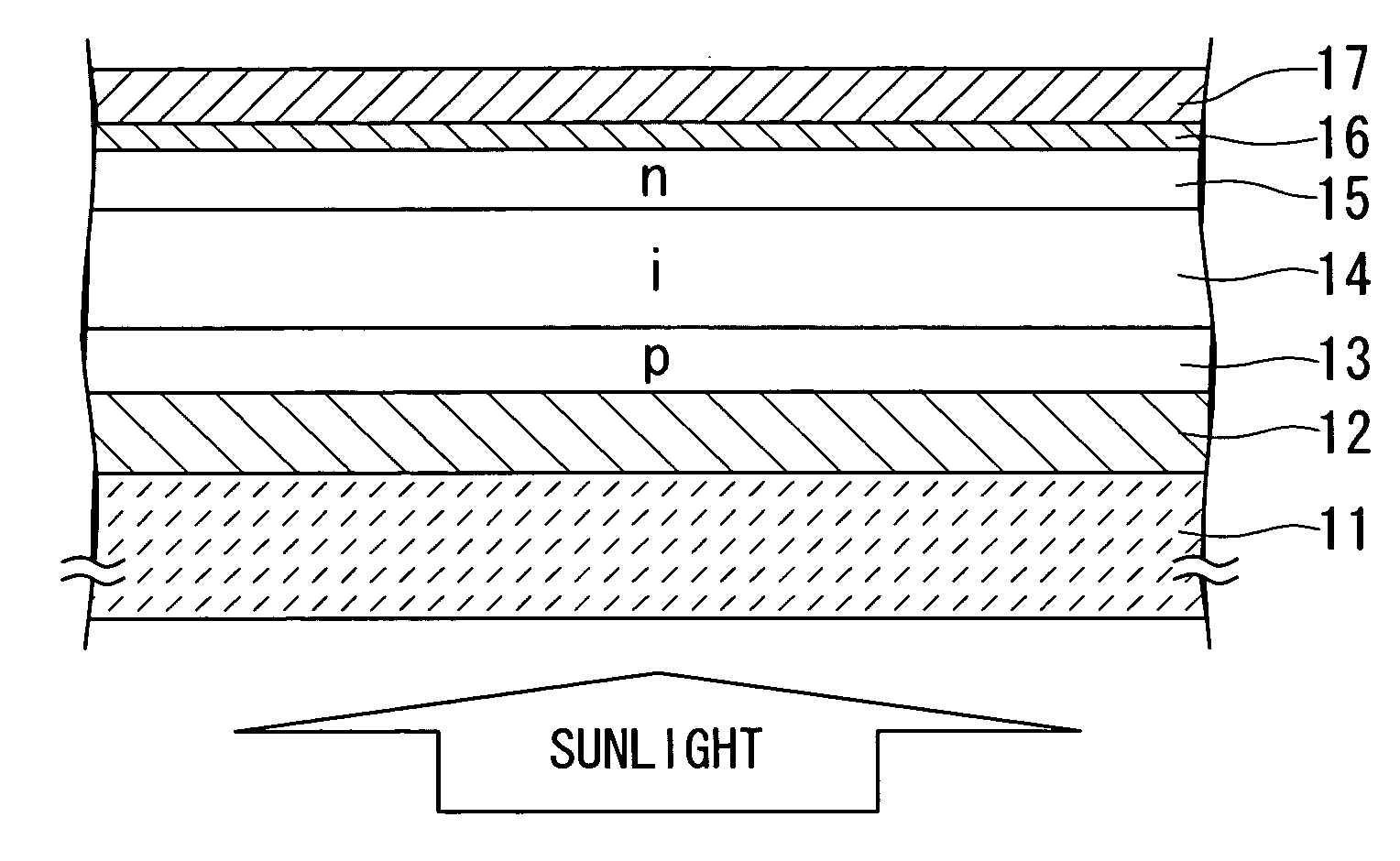
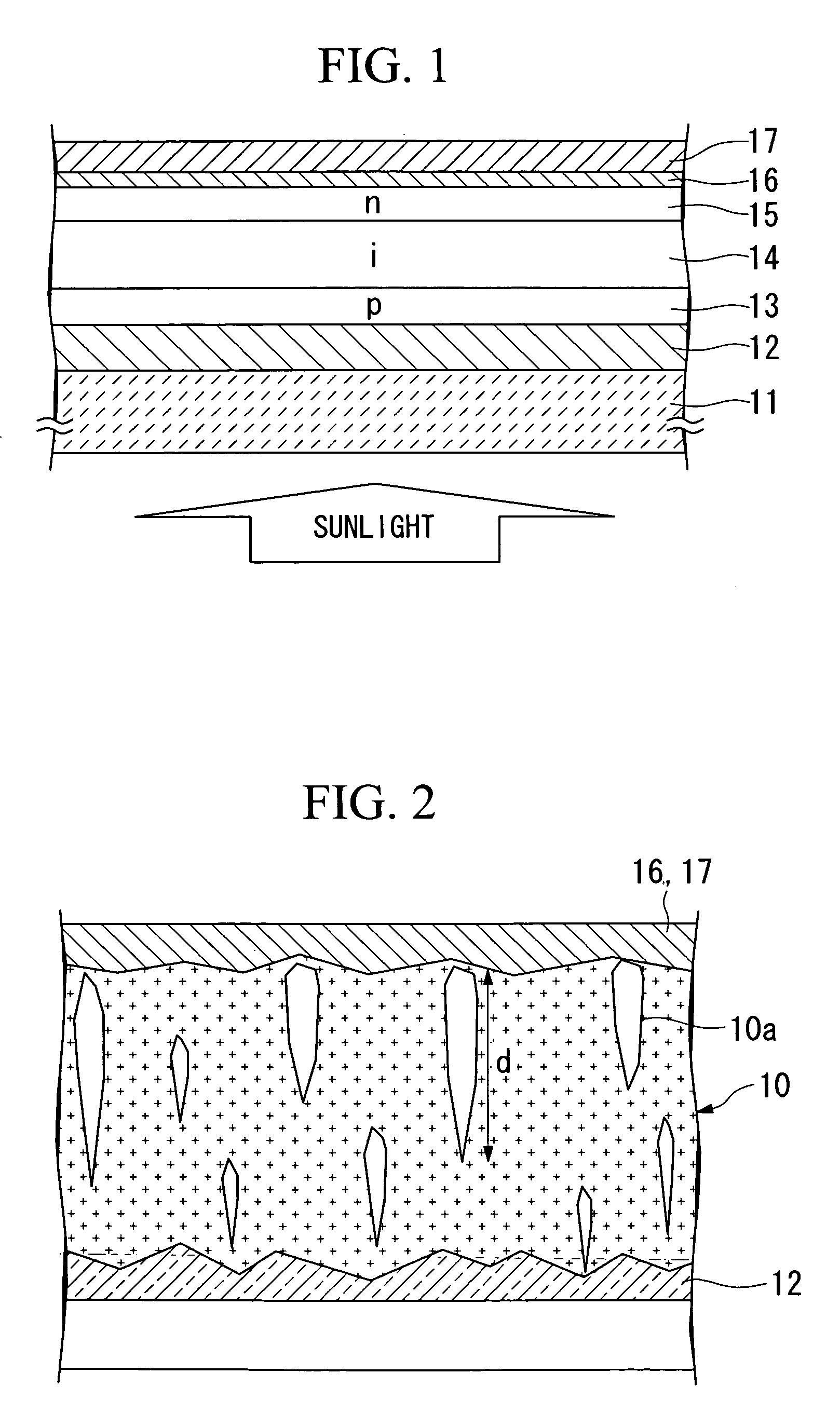
[0064] A process according to the present invention for producing the type of solar cell into which light enters through the electrically insulating substrate side will be described with reference to FIG. 1.

First Step

[0065] A first transparent electrode (first electrode) 12 is formed on an electrically insulating transparent substrate (electrically insulating substrate) 11. Optically transparent white crown glass, for example, can be used for the electrically insulating transparent substrate 11. The first transparent electrode 12 is made of a metal oxide such as tin oxide (SnO2) or zinc oxide (ZnO). In order to prevent the first transparent electrode 12 from being reduced by hydrogen used in the production step of polycrystalline silicon layers as explained below, a zinc oxide film with a thickness of several tens of nanometers may be formed on the first transparent electrode 12.

Second Step

[0066] Subsequently, while the electrically insulating transparent substrate 11 on which...

second embodiment

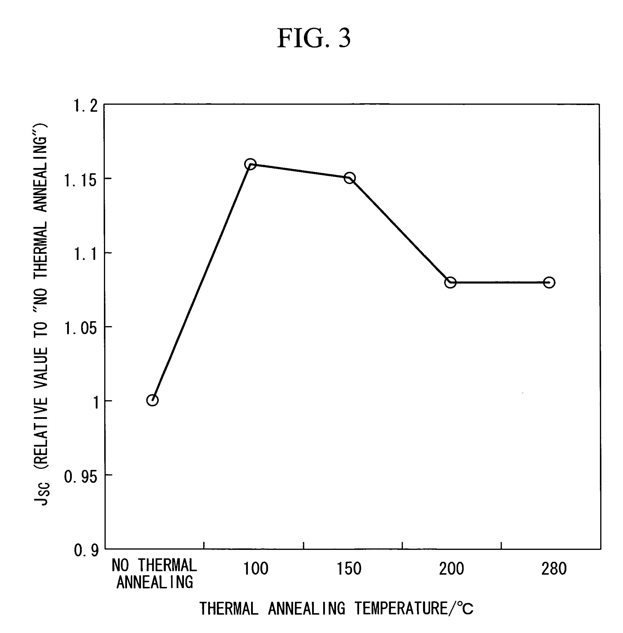
[0082] Next, a process for producing a solar cell will be described as a second embodiment of the present invention. The process for producing a solar cell according to the second embodiment differs from that according to the first embodiment explained above in that thermal annealing of the p-type or n-type silicon layer after formation of the first transparent electrode is carried out in a low-pressure oxygen atmosphere. Therefore, the step of thermal annealing in oxidation atmosphere of the p-type or n-type silicon layer will be described in detail for the second embodiment, whereas detailed description of the other steps, which are similar to those in the first embodiment, will be omitted.

[0083] In the first step, a first transparent electrode (first electrode) is formed on an electrically insulating transparent substrate (electrically insulating substrate). Then, in the second step, a polycrystalline p-type silicon layer is formed on the first transparent electrode using a plas...

third embodiment

[0097] A process according to the present invention for producing the type of solar cell into which light enters through the second transparent electrode side will be described with reference to FIG. 16.

First Step

[0098] A back electrode 18 made, for example, of Al or Ag is formed on a electrically insulating transparent substrate 11 (electrically insulating substrate) made, for example, of optically transparent white crown glass. Then, a first transparent electrode 19 made of a metal oxide such as zinc oxide (ZnO) or indium tin oxide (ITO) is formed on the back electrode 18.

Second Step

[0099] Subsequently, while the electrically insulating transparent substrate 11 on which the first transparent electrode 19 is formed is held as a processing object on an anode of a plasma enhanced CVD apparatus, the processing object is housed in a reaction chamber, which is then evacuated to a vacuum using a vacuum pump. Then, electricity to a heater incorporated in the anode is turned on, and ...


PUM

PropertyMeasurementUnit
temperatureaaaaaaaaaa

Abstract

A process for producing a solar cell is provided which can enhance the photovoltaic conversion efficiency by enlarging the grain sizes in the direction of the thickness of an i-layer to reduce grain boundaries, thereby avoiding recombination of carriers and activating the dopant at the same time. A process for producing a solar cell includes depositing at least a first transparent electrode, polycrystalline silicon layers in a PIN structure, and a second electrode in sequence on an electrically insulating substrate, the polycrystalline silicon layers in a PIN structure including a p-type silicon layer, an i-type silicon layer, and an n-type silicon layer, wherein the polycrystalline silicon layers in a PIN structure are formed by: forming a p-type, which is then subjected to thermal annealing; depositing an i-type silicon layer on the p-type silicon layer; and depositing an n-type silicon layer on the i-type silicon layer.

Description

BACKGROUND OF THE INVENTION [0001] 1. Field of the Invention [0002] The present invention relates to solar cells and to processes for producing solar cells. In particular, the present invention relates to thin film silicon-type solar cells and to processes for producing crystalline silicon-type solar cells. [0003] Priority is claimed on Japanese Patent Application No. 2003-366602, filed Oct. 27, 2003, the content of which is incorporated herein by reference. [0004] 2. Description of Related Art [0005] Use of solar cells which use amorphous silicon has begun in small scale electricity generation such as in watches, small calculators, and streetlights, followed by uses for electric power for industries and houses. However, there still remain obstacles to be overcome such as low conversion efficiency, in comparison with solar cells of bulk silicon types such as a single crystal or a polycrystal, and degradation. Such obstacles are considered as disadvantages of amorphous silicon solar ...

Claims


Application Information

Patent Timeline
Patent Type & Authority Applications(United States)
IPC IPC(8): H01L31/036H01L31/0368H01L31/0376H01L31/06H01L31/075H01L31/076H01L31/18H01L31/20
CPCH01L31/03682Y02E10/546H01L31/182Y02E10/548Y02P70/50
Inventor SANEYUKI, GOYAYOUJI, NAKANOYOSHIKI, MIYAMOTO
Owner MITSUBISHI HEAVY IND LTD
Why Eureka
Try Eureka