System for detection of wafer defects

a technology of optical inspection and wafer, applied in the direction of electromagnetic transmission, instruments, transmission, etc., can solve the problems of reducing wafer throughput, affecting the transmission efficiency of the system, and affecting the detection efficiency of the system. , to achieve the effect of reducing the transmission loss

Inactive Publication Date: 2005-05-26
APPLIED MATERIALS SOUTH EAST ASIA PTE
View PDF89 Cites 38 Cited by
  • Summary
  • Abstract
  • Description
  • Claims
  • Application Information

AI Technical Summary

Benefits of technology

[0081] In accordance with still a further preferred embodiment of the present invention, there is also provided a method of reducing the transmission loss in a fiber optical bundle for reducing the coherence of light transmitted therethrough, at least part of which light has a characteristic coherence length, the method comprising the steps of providing ...

Problems solved by technology

Fabrication of semiconductor wafers is highly complex and very expensive, and the miniature integrated circuit patterns of semiconductor wafers are highly sensitive to process induced defects, foreign material particulates, and equipment malfunctions.
Therefore, advanced semiconductor wafers are vulnerable to smaller sized defects than are currently detected.
Scanning a given sized wafer using increasingly smaller pixel sizes causes a corresponding increase in per wafer inspection time, resulting in decreased wafer throughput, and decreased statistical sampling in terms of the number of inspected wafers.
Conversely, attempting to increase wafer inspection throughput by using current optical system pixel sizes results in reducing the effectiveness, i.e., resolution, of wafer defect detection.
Fabricating 12-inch wafers is significantly more expensive than fabricating 8-inch wafers.
In particular, costs of raw materials of 12-inch wafers are higher than those of 8-inch wafers.
However, inspection speed, and consequently, wafer throughput of these systems became technology limited and didn't keep up with increasingly stringent production requirements, i.e., fabricating integrated circuit chips from wafers of increasing size and decreasing critical dimensions.
This is a relatively slow process, and as a result, quantity of on-line inspection data acquired during a manufacturing process is small, generating a relatively small statistical sample of inspected wafers, translating to relatively long times required to detect wafer fabrication problems.
Slow systems of on-line defect detection result in considerable wafer scrap, low wafer production yields, and overall long turn-around-times for pin-pointing fabrication processing steps and/or equipment causing wafer defects.
A notable limitation of current methods and systems of wafer defect detection relates to registration of pixel positions in ...

Method used


Image

  • System for detection of wafer defects
  • System for detection of wafer defects
  • System for detection of wafer defects

Examples


Embodiment Construction

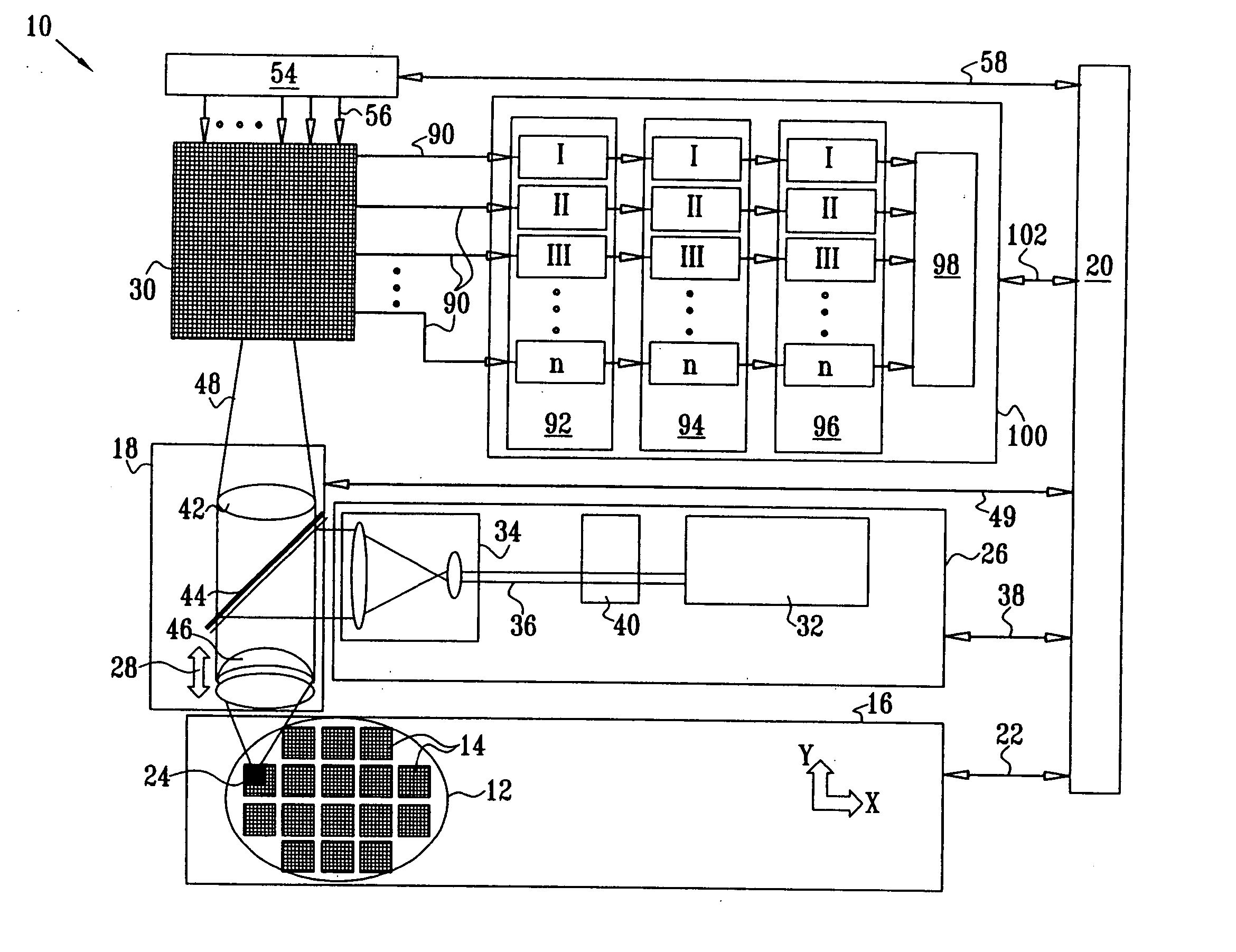
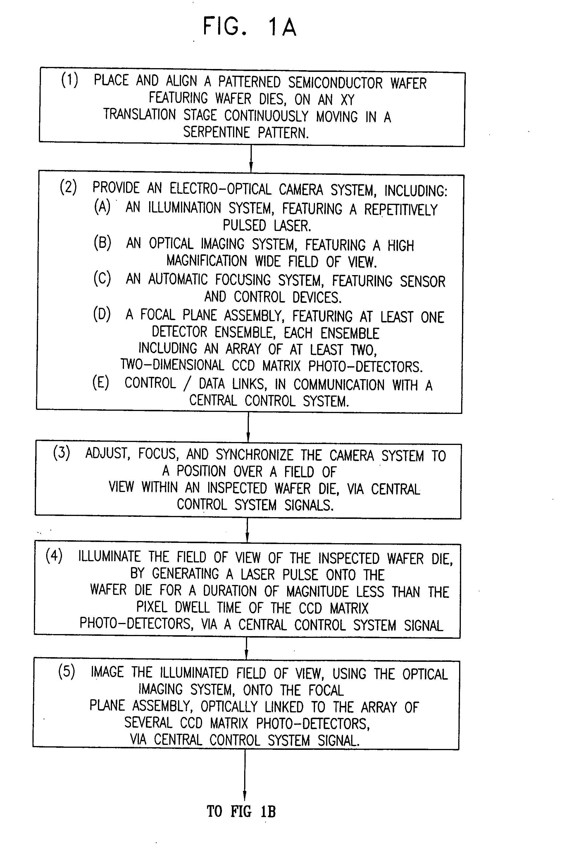
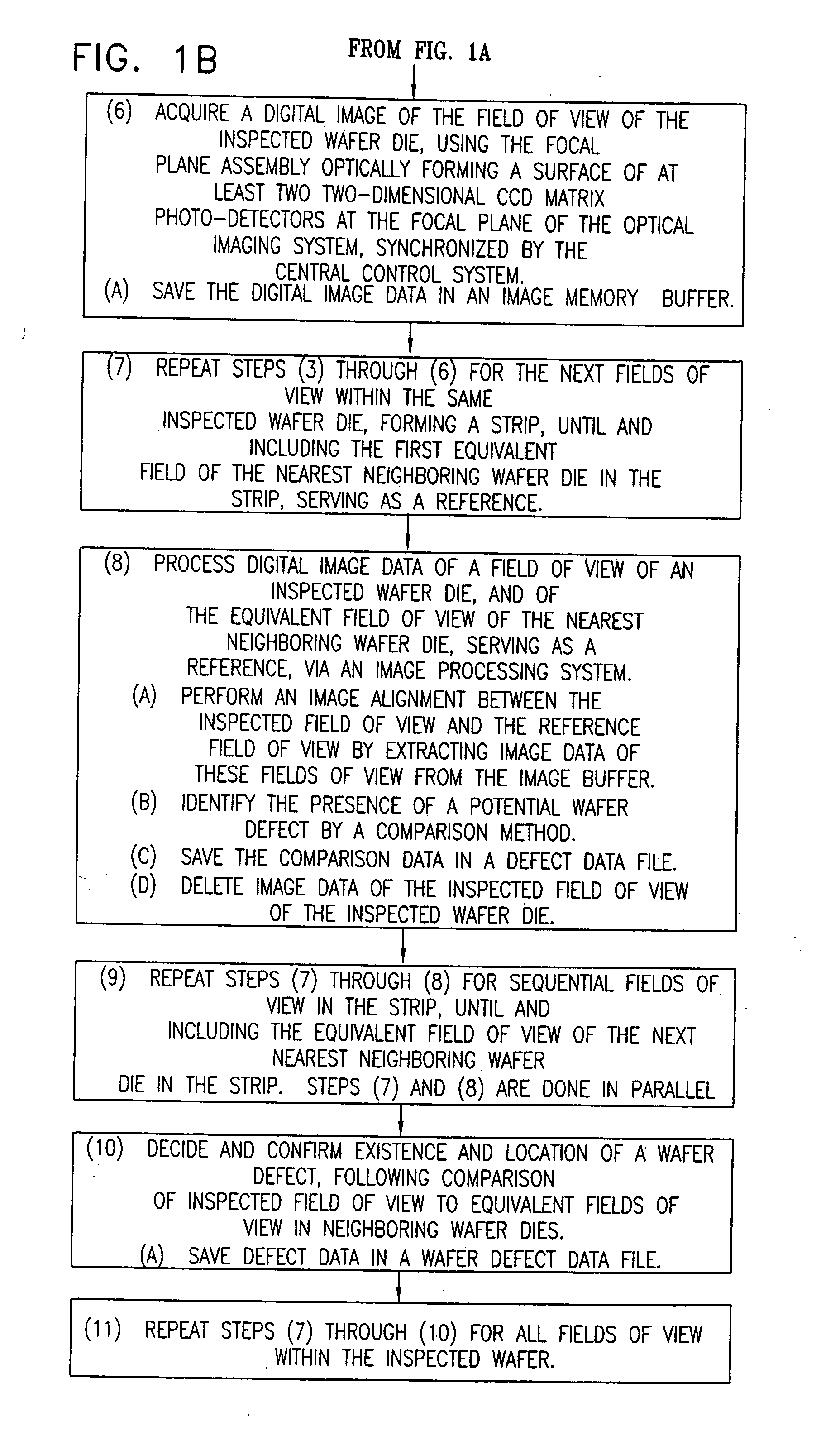
[0126] The present invention provides a method and system for fast on-line electro-optical detection of wafer defects.

[0127] The method and system for fast on-line electro-optical detection of wafer defects of the present invention introduces the unique combination of a new imaging system featuring an optically formed surface of photo-detectors at the focal plane formed from an array of several two-dimensional matrix photo-detectors for acquiring a high resolution, high pixel density, large field of view image of a wafer die, synchronized with an illumination system featuring illumination of the wafer die by a short light pulse from a repetitively pulsed laser. The laser light pulse duration is significantly shorter than the image pixel dwell time, where the pixel dwell time refers to the time a point on the wafer is imaged by a detector pixel while the wafer is moving, and the laser light pulse rate is synchronized with the frame speed of the individual matrix photo-detectors.

[01...


PUM


Abstract

Fast on-line electro-optical detection of wafer defects by illuminating with a short light pulse from a repetitively pulsed laser, a section of the wafer while it is moved across the field of view of an imaging system, and imaging the moving wafer onto a focal plane assembly, optically forming a continuous surface of photo-detectors at the focal plane of the optical imaging system. The continuously moving wafer is illuminated by a laser pulse of duration significantly shorter than the pixel dwell time, such that there is effectively no image smear during the wafer motion. The laser pulse has sufficient energy and brightness to impart the necessary illumination to each sequentially inspected field of view required for creating an image of the inspected wafer die. A novel fiber optical illumination delivery system, which is effective in reducing the effects of source coherence is described. Other novel aspects of the system include a system for compensating for variations in the pulse energy of a Q-switched laser output, methods for autofocussing of the wafer imaging system, and novel methods for removal of repetitive features of the image by means of Fourier plane filtering, to enable easier detection of wafer defects.

Description

FIELD OF THE INVENTION [0001] The present invention relates to methods and systems for the optical inspection of objects for defects, and in particular, for optically detecting random fabrication defects in semiconductor patterned structures such as integrated circuit dies or chips. BACKGROUND OF THE INVENTION [0002] Current methods and systems of defect detection on wafers are usually based on comparisons of signals obtained from inspection of a number of adjacent wafer dies or fields of view, featuring a like pattern. Defects produced during wafer fabrication are assumed to be random in nature. Therefore, defect detection is based on a statistical approach, whereby the probability that an identical random defect will be present at the same location within adjacent wafer dies is very low. Hence, defect detection is commonly based on identifying irregularities through the use of the well known method of die-to-die comparison. [0003] A given inspection system is programmed to inspect...

Claims


Application Information

Patent Timeline
IPC IPC(8): G01NG01N1/00G01N21/88G01N21/95G01N21/956H01L21/20H01L21/66H04B10/08
CPCG01N21/8806G01N21/9501G01N21/95607G01N2201/0826G01N2021/479G01N2021/8825G01N2201/0697G01N21/95623H01L21/20H01L22/00
Inventor FURMAN, DOVNEUMANN, GADWAGNER, MARKDOTAN, NOAMSEGAL, RAMSILBERSTEIN, SHAI
Owner APPLIED MATERIALS SOUTH EAST ASIA PTE
Why Eureka
Try Eureka