Selectively adherent substrate and method for producing the same
- Summary
- Abstract
- Description
- Claims
- Application Information
AI Technical Summary
Benefits of technology
Problems solved by technology
Method used
Image
Examples
first embodiment
[0058] Materials used for the substrate of the present invention includes glass, ceramics, semiconductor, metal, resin and the lice. Types or glass usable include a quartz glass (coefficient of linear expansion α=0.5 ppm / K), a non-alkali glass, a soda-lime glass and the like. Further included are a low expansion glass ceramics such as Zerodur (SCHOTT, α=−2 ppm / K), NEOCERAM (Nippon Electric Glass, α=0.15 ppm / K) and the like, pyrex (Corning, α=3.25 ppm / K) BK7 (SCHOTT, α=7.1 ppm / K) and others.
[0059] Furthermore, a silicon provided in the form of wafer and a semiconductor such as InP, GaAs and the like are also available. Resin materials include an epoxy resin, an acrylic resin, a polycarbonate resin, a polyimide resin, a fluoric resin and the like. Even among these, it is most preferable to use a glass which is superior in heat resistance, transparency and chemical stability.
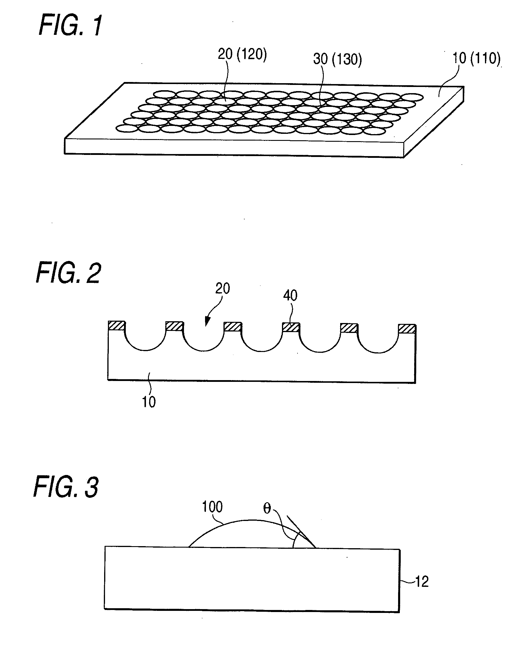
[0060] One embodiment of the selectively adherent substrate of the present invention is shown in FIG. 1. On th...
example 1
[0090] (Preparation of Coating Solution for a Water Repellent Layer)
[0091] The coating solution for water repellent layer (hereinafter, the solution is referred to as Liquid A) was prepared by mixing an ethanol (97.68 parts by weight), heptadecafluorodecyltrimethoxysilane (0.02 parts by weight), tetraethoxysilane (0.3 parts by weight) and concentrated sulfuric acid (2.0 parts by weight), followed by stirring for 30 minutes at a room temperature.
[0092] (Substrate Manufacturing)
[0093] Liquid A was coated on the quartz glass substrate (thickness 2 mm, size 50 mm×50 mm) by a spin-coating method. After being dried for 24 hours at a room temperature, Cr film and AU film were formed by a spattering method, followed by photoresist coating by a spin-coating method. Thereafter, the photoresist film was exposed with a pattern having apertures of 2500 in total arranged in a grid pattern such as 50 in the longitudinal direction and 50 in the transverse direction, followed by developing and th...
example 2
[0099] Cr film and AU film were formed by a spattering method on the quartz glass substrate (thickness 2 m=, size 50 mm×50 mm), followed by photoresist coating by a spin-coating method. Thereafter, the photoresist film was exposed with a pattern having apertures of 2500 in total arranged in a grid pattern such as 50 in the longitudinal direction and 50 in the transverse direction, followed by developing and then removing the exposed parts of the photoresist. Au film and Cr film were etched by using the photoresist film as a mask to form apertures.
[0100] The glass substrate with the mask was washed with ultra pure water (specific resistance: 18MΩ·cm) followed by etching with 49% hydrofluoric acid. Thereafter, the photoresist film was peeled off by NaOH aqueous solution after being washed by ultra pure water. Furthermore, Cr film was peeled away by using an aqueous solution of nitric acid diammonium cerium after the Au mask was peeled away by using an aqueous solution of iodine / ammon...
PUM
 Abstract
Description
Claims
Application Information


