Surface acoustic wave element and electronic equipment
a surface acoustic wave element and electronic equipment technology, applied in piezoelectric/electrostrictive/magnetostrictive devices, piezoelectric/electrostriction/magnetostriction machines, electrical apparatus, etc., can solve the problems of small size, distortion of piezoelectric substrates by electric fields, and miniaturization of surface acoustic wave elements. achieve high reliability
- Summary
- Abstract
- Description
- Claims
- Application Information
AI Technical Summary
Benefits of technology
Problems solved by technology
Method used
Image

Examples
first embodiment
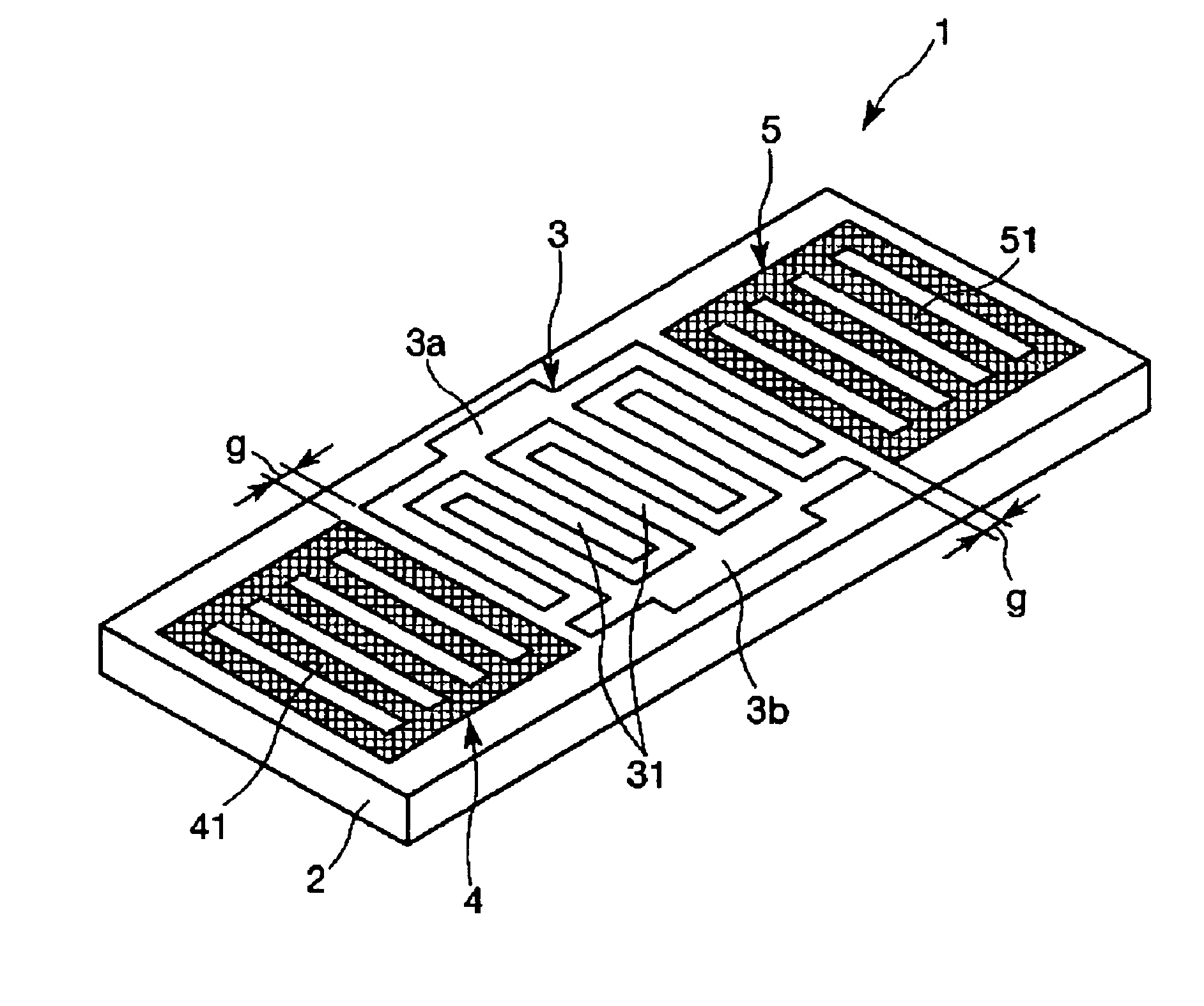
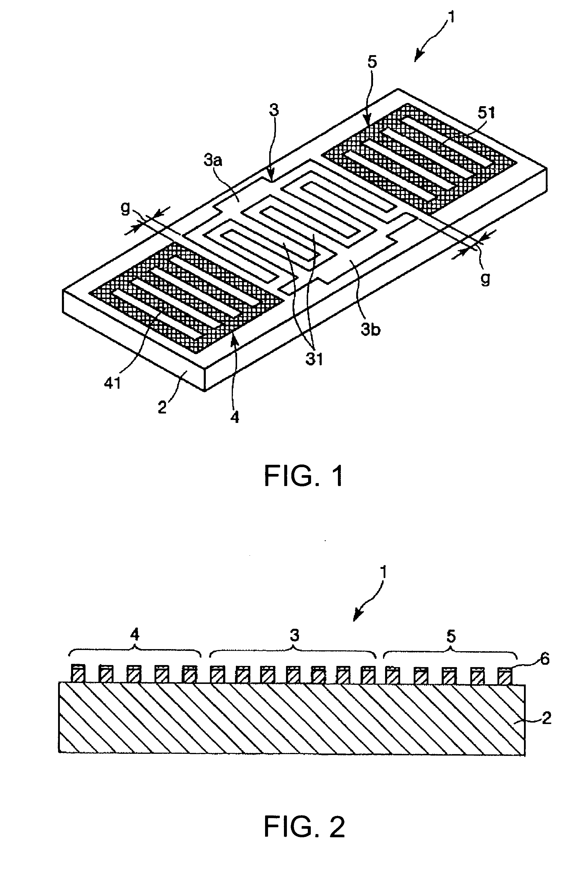
[0046]FIG. 1 is a perspective view schematically showing a first embodiment of the surface acoustic wave element of the present invention, and FIG. 2 is a cross sectional view of the surface acoustic wave element shown in FIG. 1. In addition, in the following description, the upper side in FIG. 2 is called a “top” and the lower side is called a “bottom”.
[0047] The surface acoustic wave element 1 shown in FIG. 1 and FIG. 2 has a substrate 2, an IDT 3 provided on the substrate 2, a pair of reflectors 4 and 5 arranged at both side portions of the IDT 3, an insulating protection film 6 provided in the top face of the IDT 3 and the reflectors 4 and 5.
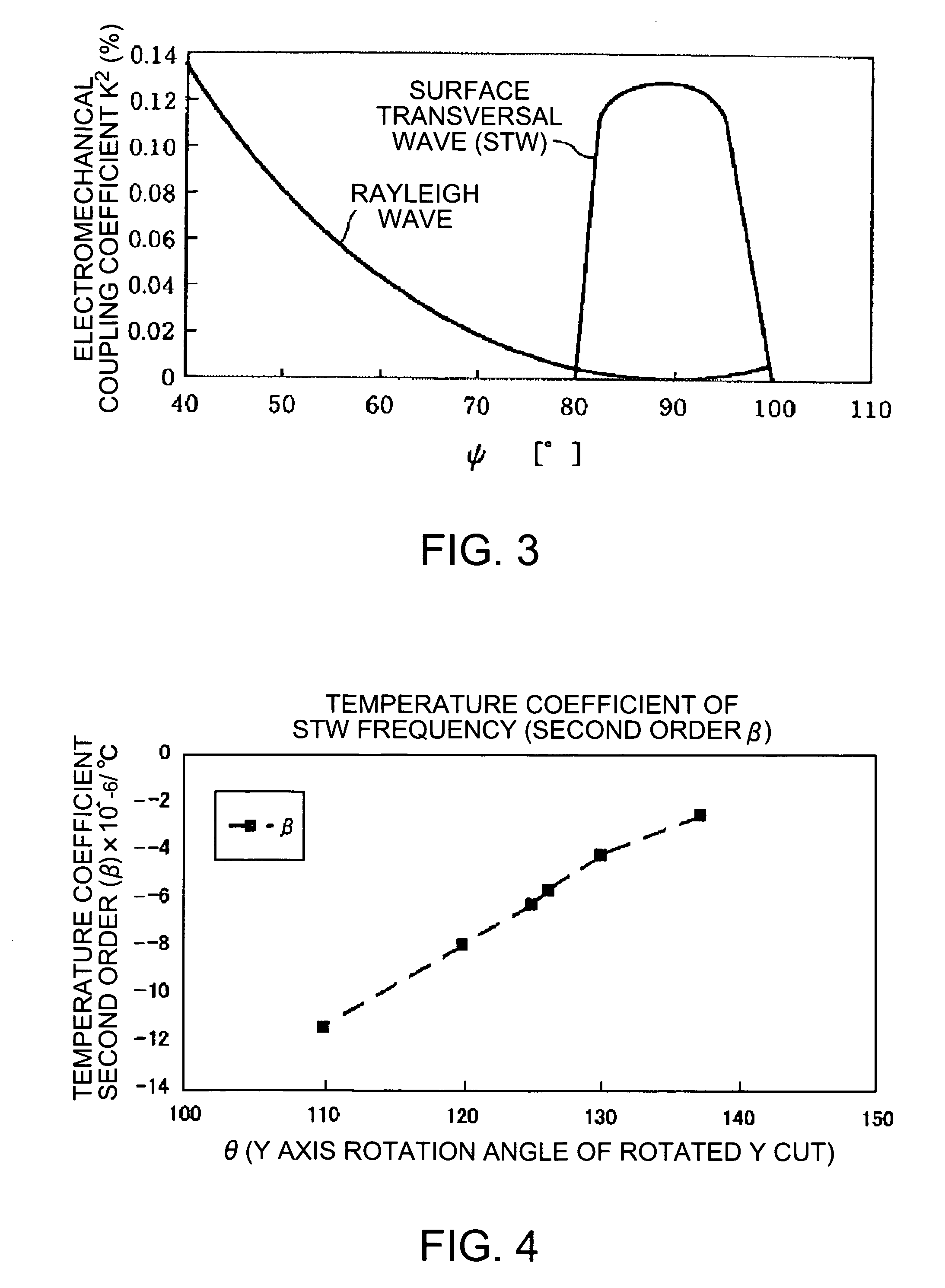
[0048] In the present invention, a quartz-rotator Y plate is used as the substrate 2. Accordingly, in the surface acoustic wave element 1, a surface acoustic wave with a large electromechanical coupling coefficient k2 is excited.
[0049] The present invention prescribes the angle ψ and the cut angle θ of the Euler angle (0, θ, ψ) in this qu...
second embodiment
[0093] Next, a second embodiment of the surface acoustic wave element according to the present invention will be described.
[0094]FIG. 6 is a perspective view showing the second embodiment of the surface acoustic wave element of the present invention, and FIG. 7 is a cross sectional view of the surface acoustic wave element shown in FIG. 6. In addition, in the following description, an upper side in FIG. 7 is called a “top”, and a lower side is called a “bottom.”
[0095] Hereinafter, the surface acoustic wave element of the second embodiment will be described focusing on differences from the surface acoustic wave element 1 of the first embodiment, and the description regarding the same matters will be omitted.
[0096] A surface acoustic wave element 7 of the second embodiment is the same as the surface acoustic wave element 1 of the first embodiment except that an IDT 8 used for an input and an IDT 9 used for an output are provided, respectively, instead of the IDT 3 having the combine...
embodiment 1
[0124] First of all, as the substrate, a quartz-rotator Y plate whose average thickness is 0.4 mm is prepared. The Euler angle of this quartz-rotator Y plate is (0, 133, 90).
[0125] Aluminum is adhered on this quartz-rotator Y plate to form a conductive material layer preferably by a vacuum deposition method or a sputtering method.
[0126] Next, silicon oxide (SiO2) is adhered on this conductive material layer to form a silicon oxide layer (insulating material layer) whose average thickness is about 40 nm by a CVD method or a sputtering method.
[0127] Then, a resist layer with the shape corresponding to the IDT (interdigital transducer) and the reflectors is formed on the silicon oxide layer by a photo lithography method.
[0128] Then, the unwanted conductive material layer and silicon oxide layer are removed by a dry etching method using this resist layer as a mask. Thereby, the IDT, the reflectors, and the insulating protection film are formed, and the surface acoustic wave element ...
PUM
 Abstract
Description
Claims
Application Information
 - R&D
- Intellectual Property
- Life Sciences
- Materials
- Tech Scout
- Unparalleled Data Quality
- Higher Quality Content
- 60% Fewer Hallucinations
Browse by: Latest US Patents, China's latest patents, Technical Efficacy Thesaurus, Application Domain, Technology Topic, Popular Technical Reports.
© 2025 PatSnap. All rights reserved.Legal|Privacy policy|Modern Slavery Act Transparency Statement|Sitemap|About US| Contact US: help@patsnap.com