Semiconductor device and fabrication method thereof

a technology of semiconductor devices and capacitors, which is applied in the direction of basic electric elements, transportation and packaging, vehicle arrangements, etc., can solve the problems of deterioration of ferroelectric materials, deterioration of performance of ferroelectric capacitors, and formation of oxygen defects in ferroelectric films, so as to prevent the occurrence of defects by prevent the effect of deterioration of device performance and deterioration of ferroelectric capacitors

Active Publication Date: 2005-06-16
FUJITSU SEMICON LTD
View PDF5 Cites 68 Cited by
  • Summary
  • Abstract
  • Description
  • Claims
  • Application Information

AI Technical Summary

Benefits of technology

[0015] Accordingly, the present invention has been made in view of the foregoing problems and has the object of providing a semiconductor device having improved reliability over a long period of time by effectively eliminating the performance degradation caused by penetration of moisture and further a fabrication process of such a semiconductor device.
[0016] Another and more specific object of the present invention is to provide a semiconductor device having a ferroelectric capacitor in which degradation of the ferroelectric capacitor caused by penetration of water is effectively suppressed.
[0019] According to the present invention, it becomes possible to block the moisture penetrating from the electrode pad by forming the guard ring between the electrode pad and the circuit part so as to surround the circuit part substantially. Thereby, deterioration of performance is successfully avoided for the elements formed in the circuit part, particularly the ferroelectric capacitor formed in the circuit part.
[0021] According to the present invention, the moisture invading into the semiconductor device from outside through the surface thereof is completely blocked by providing the barrier layer on the interlayer insulation film covering the ferroelectric capacitor and further providing the insulating metal oxide film on the barrier layer. Thereby, the problem of the invaded moisture reaching the ferroelectric capacitor is effectively prevented.
[0023] According to the present invention, penetration of moisture through the inner wall surface of the opening is presented by covering the entirety of the sidewall surface of the opening formed in the passivation film so as to expose the electrode pad. Thereby, occurrence of defect by deterioration of the ferroelectric capacitor is prevented effectively even in the case the semiconductor device is subjected to a PTHS test and held under a stressed environment of high temperature, high humidity and high pressure.
[0024] Thus, according to the present invention, penetration of water from the surface and sidewall surface of the semiconductor device, particularly from the electrode pad or the region surrounding the electrode pad is blocked effectively, and deterioration of device performance, particularly the deterioration of the ferroelectric capacitor is prevented. Thereby, a semiconductor device having excellent long-term reliability is realized.

Problems solved by technology

With such a ferroelectric film, it has been known that the characteristics of the ferroelectric material are deteriorated when moisture has penetrated from outside via an interlayer insulation film such as silicon oxide film, which has high affinity to water.
More specifically, water thus penetrated into the semiconductor device undergoes decomposition into hydrogen and oxygen during the high temperature semiconductor process used at the time of formation of the interlayer insulation film or metal wiring patterns, while the hydrogen atoms thus formed cause formation of oxygen defects in the ferroelectric film as a result of causing reaction with oxygen in the ferroelectric film.
As a result, there occurs degradation of performance in the ferroelectric capacitor such as decrease of the residual dielectric polarization or decrease of the dielectric constant.
Further, there occur also the cases in which the performance of the transistors and other devices is degraded.

Method used


Image

  • Semiconductor device and fabrication method thereof
  • Semiconductor device and fabrication method thereof
  • Semiconductor device and fabrication method thereof

Examples


first embodiment

(First Embodiment)

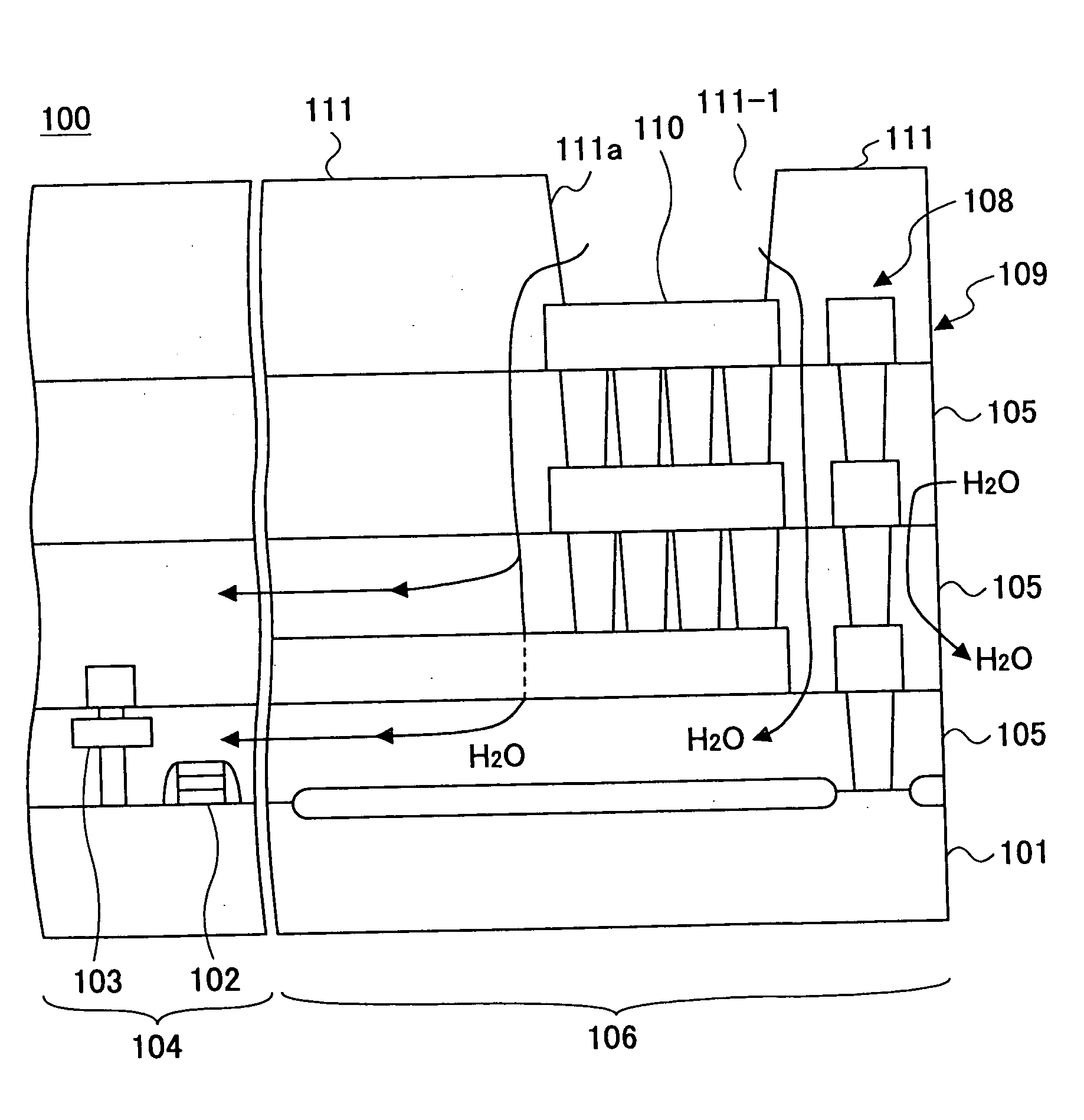
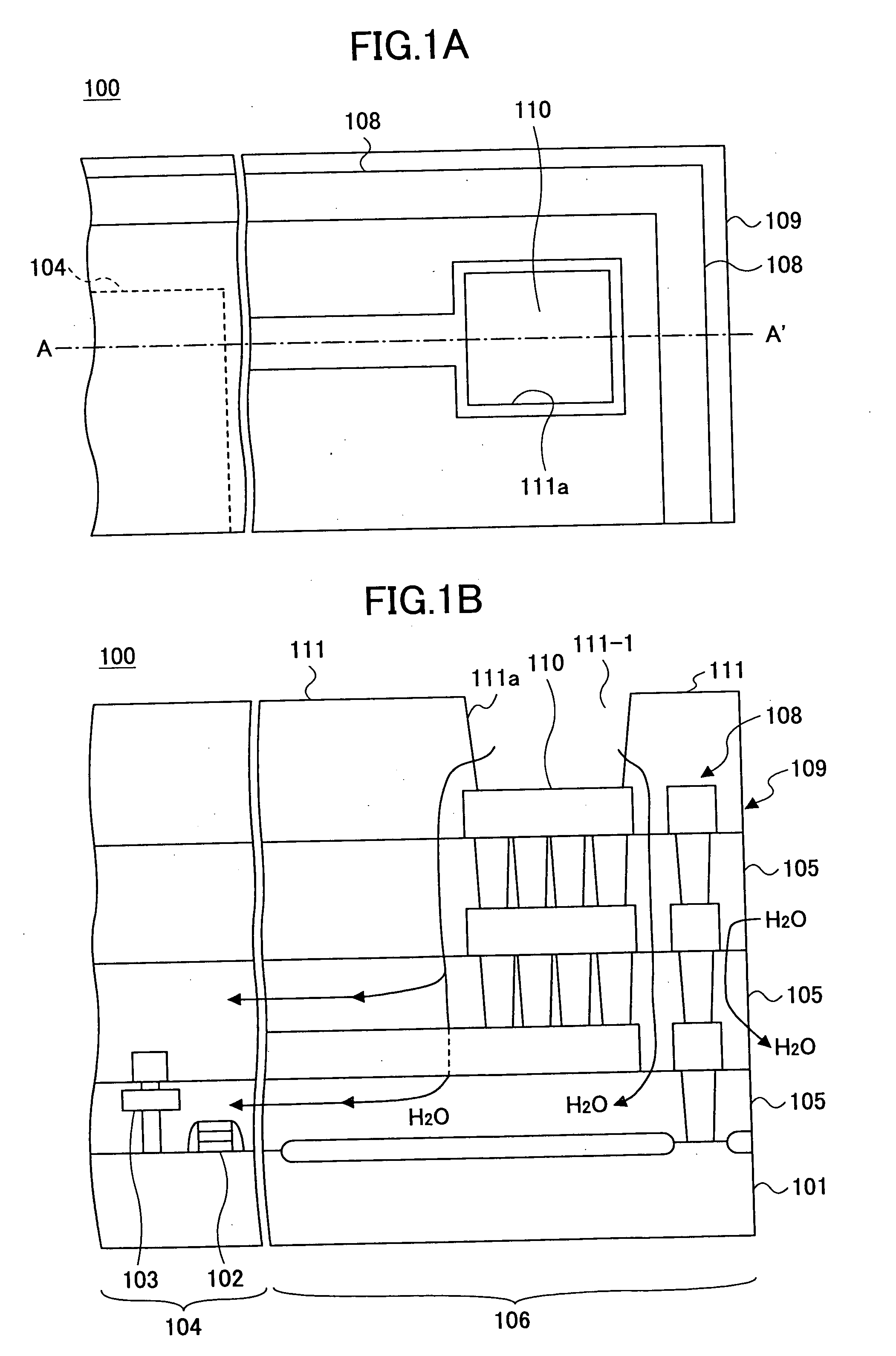
[0044]FIG. 3 is a plan view diagram showing a semiconductor device 10 according to a first embodiment of the present invention.

[0045] Referring to FIG. 3, the semiconductor device 10 is a ferroelectric random access memory and includes a circuit part 11, plural electrode pads 12, a first water-blocking guard ring 13, a second water-blocking guard ring 14, wiring patterns 15, and the like.

[0046] The circuit part 11 is formed on a semiconductor substrate to be explained later and includes transistors, ferroelectric capacitors, interconnection layers, and the like. On the other hand, the electrode pads 12 are disposed at the peripheral part 16 of the semiconductor device 10 for wire bonding to inner leads of a package not illustrated. Thereby, the terminals of the package are connected to the circuit part 11 via the plugs, conductive pads and interconnection layers inside the semiconductor device 10.

[0047] Here, it should be noted that the first water-blocking guar...

second embodiment

(Second Embodiment)

[0075]FIG. 7 is a cross-sectional diagram of a semiconductor device 50 according to a second embodiment of the present invention.

[0076] Referring to FIG. 7, the semiconductor device 50 is a ferroelectric random access memory constructed on a semiconductor substrate 51 and includes a transistor 52 formed on the semiconductor substrate 51, insulation films 53a and 53b covering the transistor 52, a ferroelectric capacitor 58 formed in the insulation film 53b and including sequential stacking of a lower electrode 54, a ferroelectric capacitor insulation film 55 and an upper electrode 56. Further, there is provided a first interlayer insulation film 59 so as to cover the ferroelectric capacitor 58 and a barrier layer 60 is formed on the first interlayer insulation film 59.

[0077] Further, an interconnection layer 62 is formed in the barrier layer 60, wherein the interconnection layer 62 includes an interconnection pattern 62a connected to a diffusion region 52a of the...

example 1

[0119] In Example 1, a ferroelectric random access memory is formed according to the process of the present invention wherein the ferroelectric random access memory of Example 1 has a structure similar to the one shown in FIG. 7.

[0120] More specifically, the ferroelectric capacitor is formed by a sputtering process to have the structure in which the Pt lower electrode 54, the PZT ferroelectric capacitor insulation film 55 and the IrO2 upper electrode 56 are stacked consecutively with respective thicknesses of 100 nm, 200 nm and 100 nm, wherein the first insulation film 59 is formed by a plasma CVD process to have the thickness of 100 nm by setting the substrate temperature to 350° C. while supplying a TEOS gas and an oxygen gas with respective flow rates of 466 SCCM and 700 SCCM under a pressure of 1.2×10³ Pa (9.0 Torr).

[0121] After formation, the first interlayer insulation film 59 is subjected to a CMP process for planarization, and the barrier layer 60 is formed further thereon...


PUM


Abstract

A semiconductor device includes a semiconductor substrate, a circuit part formed on and above the semiconductor substrate, a passivation film covering the circuit part, an electrode pad provided outside the circuit part in such a manner that the electrode pad is exposed from the passivation film, and a guard ring pattern provided between the electrode pad and the circuit part such that the guard ring pattern surrounds the circuit part substantially. The guard ring pattern extends from a surface of the semiconductor substrate to the passivation film.

Description

CROSS-REFERENCE TO RELATED APPLICATION [0001] The present application is based on Japanese priority application No.2003-413199 filed on Dec. 11, 2003, the entire contents of which are hereby incorporated by reference. BACKGROUND OF THE INVENTION [0002] The present invention relates to semiconductor devices and fabrication process thereof and more particularly to a semiconductor device having a ferroelectric capacitor and a fabrication process thereof. [0003] Intensive efforts are being made for developing a ferroelectric random access memory (FeRAM), wherein a ferroelectric random access memory is a semiconductor memory device that holds information in a ferroelectric capacitor by utilizing polarization of a ferroelectric film. A ferroelectric memory is non-volatile in that it holds the information even when electric power supplied thereto is turned off and thus attracts much attention in view of the possibility of realizing a memory device of high density integration, high speed dr...

Claims


Application Information

Patent Timeline
Patent Type & Authority Applications(United States)
IPC IPC(8): H01L21/02H01L23/52H01L21/3205H01L21/8246H01L23/00H01L23/58H01L27/10H01L27/105H01L27/115
CPCH01L23/564H01L23/585H01L2924/10253H01L27/11502H01L27/11507H01L28/40H01L2224/4912H01L2224/49171H01L2924/01046H01L2924/01057H01L2924/01077H01L2924/01078H01L2924/14H01L2924/19041H01L24/49H01L2924/00H01L2224/05554H01L2924/00014H01L2224/02166H10B53/30H10B53/00H01L2224/45099H01L2224/45015H01L2924/207B60N3/023B60Y2304/07B60Y2200/143B60Y2200/31
Inventor SAIGOH, KAORUNAGAI, KOUICHI
Owner FUJITSU SEMICON LTD
Why Eureka
Try Eureka