
Chamber cleaning method

Inactive Publication Date: 2005-07-21
TAIWAN SEMICON MFG CO LTD
View PDF7 Cites 21 Cited by
  • Summary
  • Abstract
  • Description
  • Claims
  • Application Information

AI Technical Summary

Benefits of technology

[0016] In accordance with these and other objects and advantages, the present invention is generally directed to a novel method which is suitable for cleaning the interior surfaces of a process chamber. The present invention is particularly effective in removing silicon nitride and silicon dioxide residues from the interior surfaces of a chemical vapor deposition (CVD) chamber. The method includes reacting nitrous oxide (N2O) gas with nitrogen trifluoride (NF3) gas in a plasma to generate nitric oxide (NO) and fluoride (F) radicals. Due to the increased density of nitric oxide radicals generated from the nitrous oxide, the etch and removal rate of the residues on the interior surfaces of the chamber is enhanced. Consequently, the quantity of nitrogen trifluoride necessary to efficiently and expeditiously carry out the chamber cleaning process is reduced.

Problems solved by technology

These polymer coatings frequently generate particles which inadvertently become dislodged from the surfaces and contaminate the wafers.
Furthermore, technological advances in recent years in the increasing miniaturization of semiconductor circuits necessitate correspondingly stringent control of impurities and contaminants in the plasma process chamber.
When the circuits on a wafer are submicron in size, the smallest quantity of contaminants can significantly reduce the yield of the wafers.
For instance, the presence of particles during deposition or etching of thin films can cause voids, dislocations, or short-circuits which adversely affect performance and reliability of the devices constructed with the circuits.
However, deposit of material such as silicon nitride and silicon dioxide residues on the interior surfaces of the processing chambers remains a problem.
However, these cleaning techniques are not always effective in cleaning or dislodging all the film and particle contaminants coated on the chamber walls.
The smallest quantity of contaminants remaining in the chamber after such cleaning processes can cause significant problems in subsequent manufacturing cycles.
While the cleaning efficiency of nitrogen trifluoride is satisfactory, the cost of nitrogen trifluoride is nearly four times that of fluorocarbons.
Furthermore, the etch rate of nitrogen trifluoride is relatively slow (less than about 5,000 angstroms / min. in the removal of silicon carbides and / or organosilicates from the interior surfaces of process chambers).

Method used

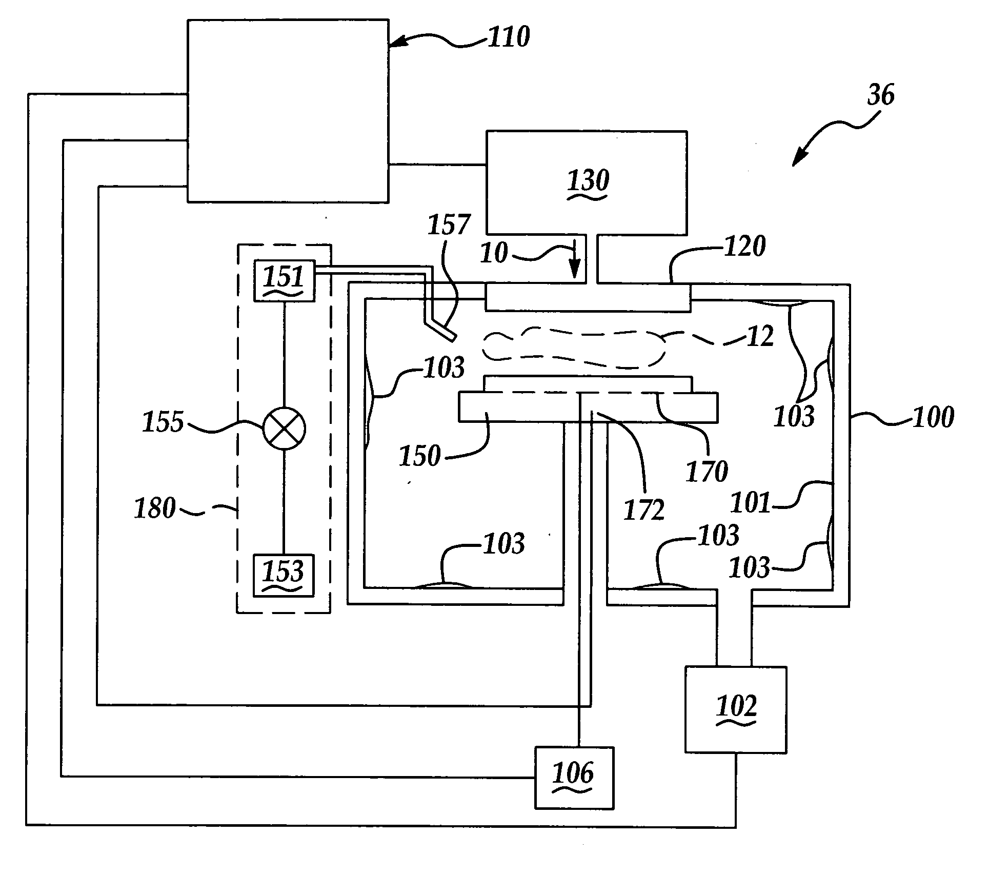
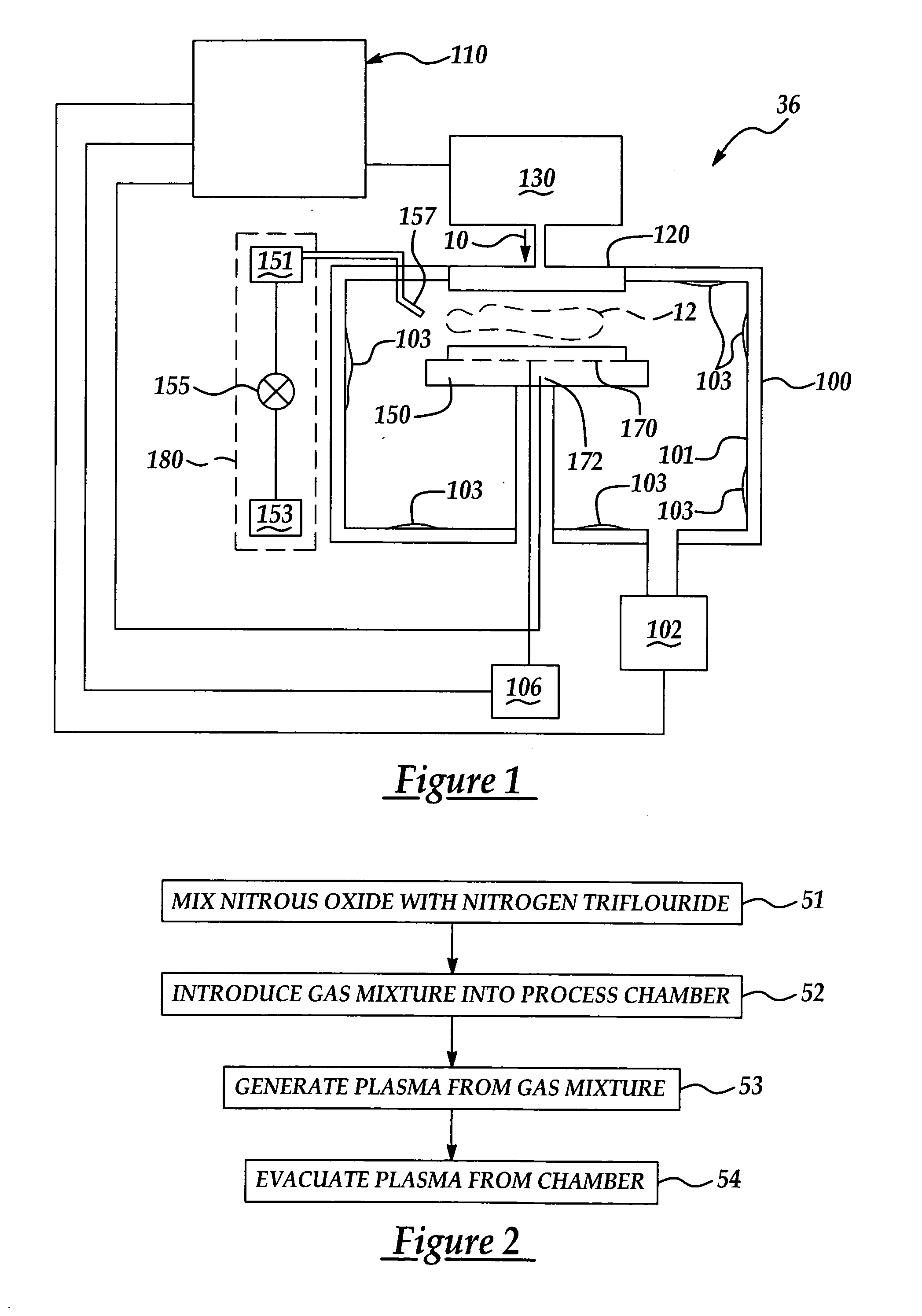
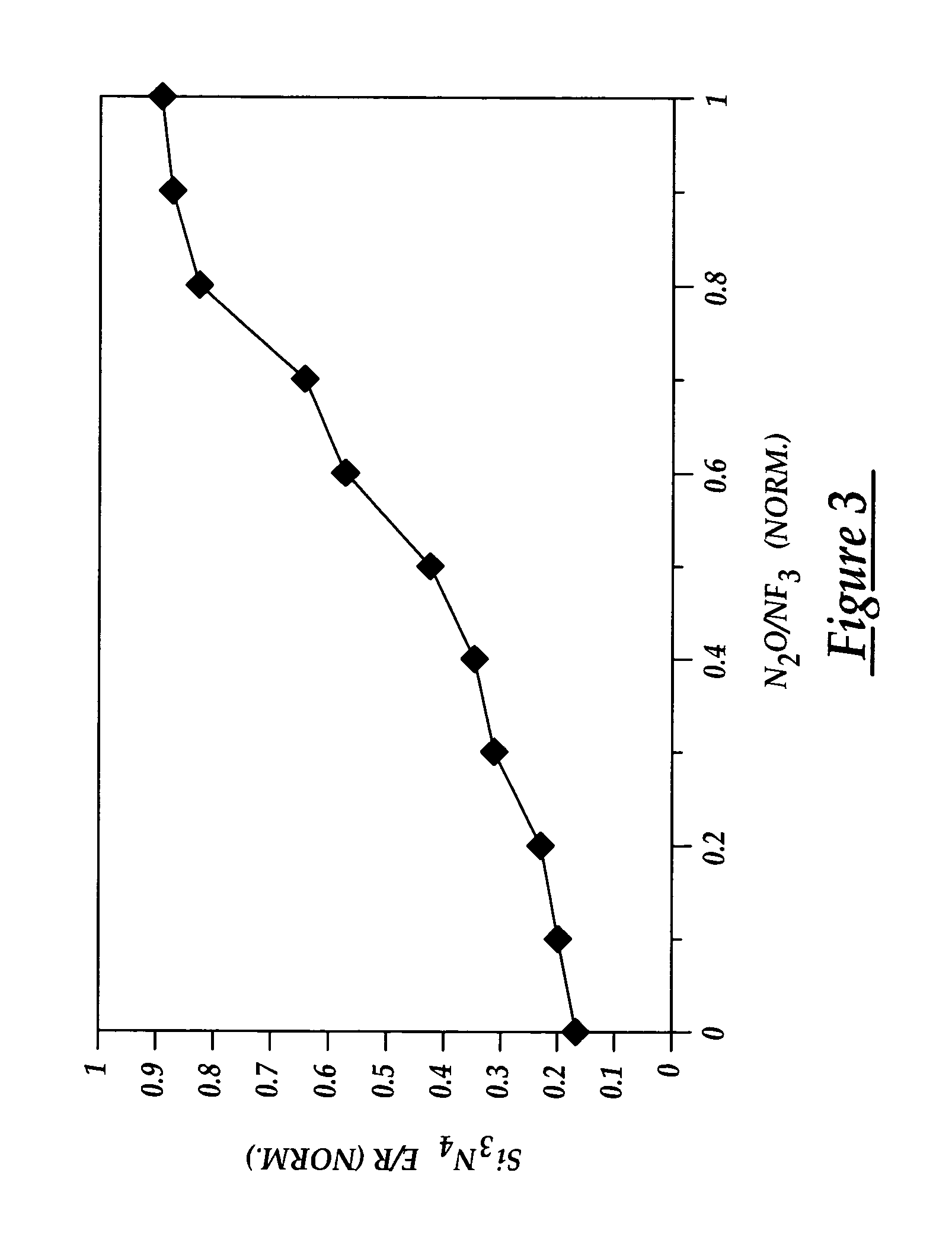

Image

  • Chamber cleaning method
  • Chamber cleaning method
  • Chamber cleaning method

Examples


Embodiment Construction

[0021] The present invention has particularly beneficial utility in the removal of material residues from the interior surfaces of a CVD process chamber used in the deposition of material layers on a semiconductor wafer substrate. However, the invention is not so limited in application, and while references may be made to such CVD process chamber, the invention is more generally applicable to removing residues from the interior surfaces of etch chambers and other process chambers used in the fabrication of integrated circuits on semiconductor wafer substrates.

[0022] The present invention contemplates a novel method suitable for cleaning the interior surfaces of a process chamber such as a chemical vapor deposition (CVD) chamber. The method includes reacting nitrous oxide (N2O) with nitrogen trifluoride (NF3) in a plasma to generate nitric oxide (NO) and fluoride (F) radicals in the process chamber. The increased density of nitric oxide radicals generated from the nitrous oxide and ...


PUM

PropertyMeasurementUnit
Densityaaaaaaaaaa
Volume ratioaaaaaaaaaa

Abstract

A method suitable for cleaning the interior surfaces of a process chamber is disclosed. The invention is particularly effective in removing silicon nitride and silicon dioxide residues from the interior surfaces of a chemical vapor deposition (CVD) chamber. The method includes reacting nitrous oxide (N2O) gas with nitrogen trifluoride (NF3) gas in a plasma to generate nitric oxide (NO) and fluoride (F) radicals. Due to the increased density of nitric oxide radicals generated from the nitrous oxide, the etch and removal rate of the residues on the interior surfaces of the chamber is enhanced. Consequently, the quantity of nitrogen trifluoride necessary to efficiently and expeditiously carry out the chamber cleaning process is reduced.

Description

FIELD OF THE INVENTION [0001] The present invention generally relates to techniques for cleaning residues from interior surfaces of a process chamber. More particularly, the present invention relates to a novel chamber cleaning method in which nitrous oxide gas is reacted with nitrogen tri-fluoride gas to generate etchant chamber-cleaning nitric oxide and fluoride radicals. BACKGROUND OF THE INVENTION [0002] In the semiconductor production industry, various processing steps are used to fabricate integrated circuits on a semiconductor wafer. These steps include the deposition of layers of different materials including metallization layers, passivation layers and insulation layers on the wafer substrate, as well as photoresist stripping and sidewall passivation polymer layer removal. In modern memory devices, for example, multiple layers of metal conductors are required for providing a multi-layer metal interconnection structure in defining a circuit on the wafer. Chemical vapor depos...

Claims


Application Information

Patent Timeline
IPC IPC(8): B08B7/00B08B7/02B08B9/00B08B9/08C23C16/44
CPCC23C16/4405B08B7/00
Inventor JANGJIAN, SHIU-KOCHEN, SHENG-WENCHANG, HUNG-JUICHANG, CHEN-LIANGWANG, YING-LANG
Owner TAIWAN SEMICON MFG CO LTD
Learn More