Semiconductor light emitting element

a technology of light-emitting elements and semiconductor layers, which is applied in the direction of basic electric elements, semiconductor devices, electrical equipment, etc., can solve the problems of electrical energy conversion efficiency or light extraction efficiency decline, and the ohmic characteristics of semiconductor layers will not necessarily be good, so as to prevent a reduction in electrical power efficiency and energy consumption , the effect of superior ohmic characteristics

Active Publication Date: 2005-07-21
NICHIA CORP
View PDF7 Cites 83 Cited by
  • Summary
  • Abstract
  • Description
  • Claims
  • Application Information

AI Technical Summary

Benefits of technology

[0046] When the semiconductor light emitting element is formed by laminating a first conductive type semiconductor layer, a light emitting layer, and a second conductive type semiconductor layer in this order, and includes electrodes that are respectively electrically connected to the first conductive type and the second conductive type semiconductor layers, and the conductive oxide film is formed on at least the second conductive type semiconductor layer, a bright light emitting element which can prevent a reduction in electrical power efficiency and which has low energy consumption can be provided because electrodes having superior ohmic characteristics can be obtained. Moreover, because the ohmic characteristics can be secured while maintaining excellent transmissivity, the light extraction efficiency can be made excellent, and a high quality and high performance light emitting element can be obtained.
[0047] When a metal film is also formed on the conductive oxide film, particularly when a single layer or laminated metal film of W, Rh, Ag, Pt, Pd, or Al is formed thereon, the Schottky barrier formed between the conductive oxide film and the metal film can be reduced, and excellent adhesiveness with the metal film can be secured regardless of whether the adhesion is performed by soldering, whether wire bonding is performed, or regardless of the form of the metal film. From amongst these, when W, Rh, or Pt are employed as the metal film, the adhesiveness with the conductive oxide film, and particu...

Problems solved by technology

However, because a conductive oxide film, e.g., ITO, exhibits n-type semiconductor characteristics, the ohmic characteristics with the semiconductor layer will not necessarily be good, and because of various factors such as the composition of semiconductor layer, the conductive type, the film formation method, and the like, a Schottky barrier will be formed, and contact resistance will increase.
Th...

Method used


Image

  • Semiconductor light emitting element
  • Semiconductor light emitting element
  • Semiconductor light emitting element

Examples


example 1

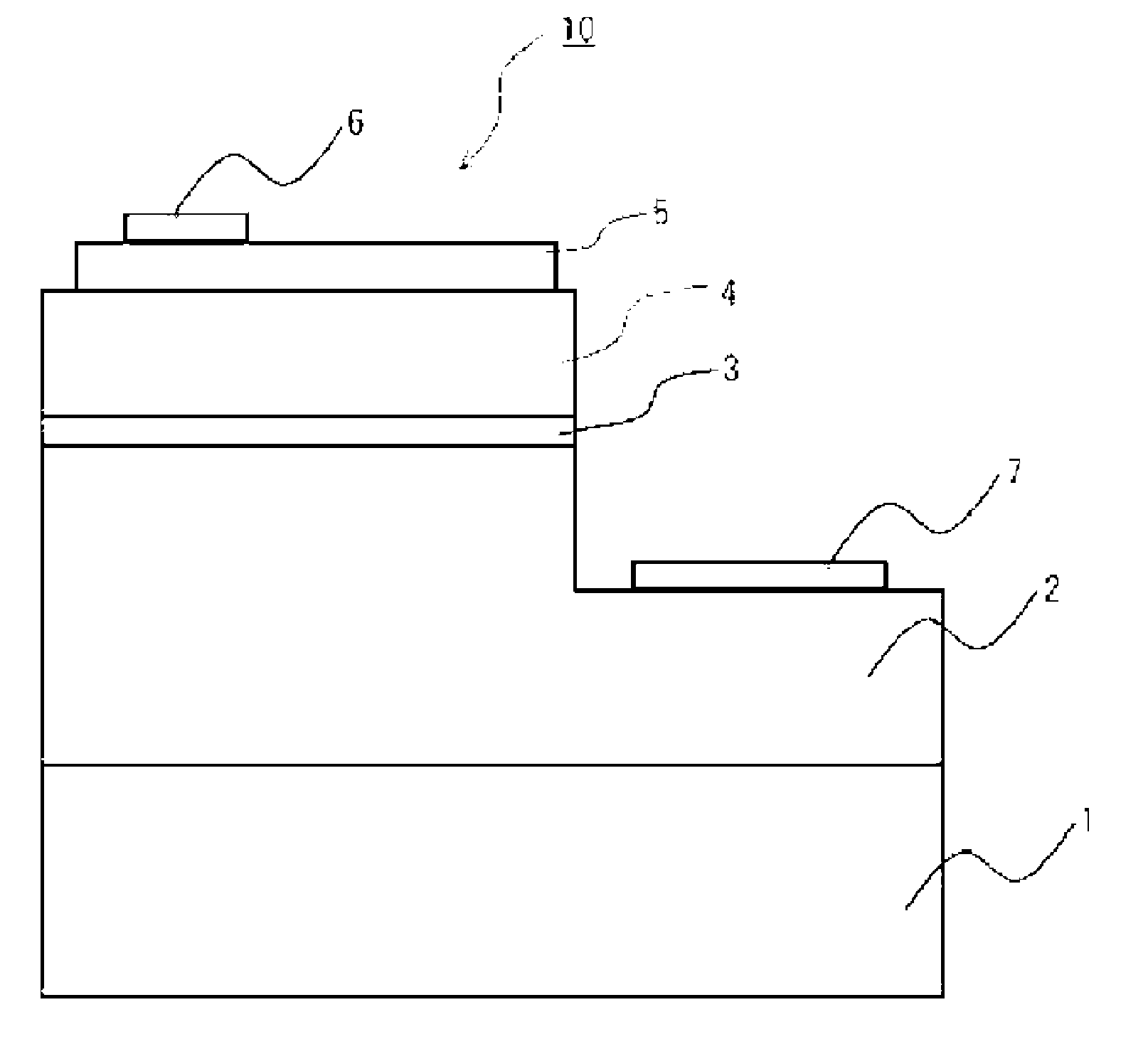
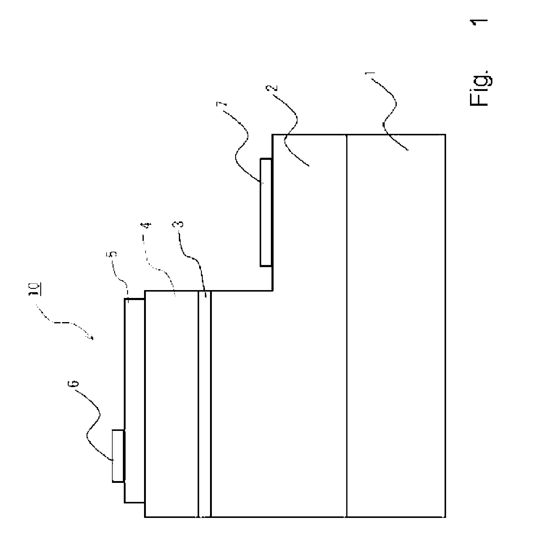
[0114] A semiconductor light emitting element of this example is shown in FIG. 1.

[0115] The semiconductor light emitting element 10 is formed by laminating, in this order, onto a sapphire substrate 1, a buffer layer (not shown in the figures) composed of Al0.1Ga0.9N, and an undoped GaN (not shown in the figures). On top of that are laminated an n-type contact layer composed of Si doped GaN as an n-type semiconductor layer 2, and a superlattice n-type clad layer in which a GaN layer (40 Å) and a InGaN layer (20 Å) are alternately laminated 10 times. On top of that are laminated an active layer 3 having a multiquantum well structure in which a GaN layer (250 Å) and an InGaN layer (30 Å) are alternately laminated 3 to 6 times, a superlattice p-type clad layer as a p-type semiconductor layer 4 in which an Al0.1Ga0.9N layer doped with Mg (40 Å) and an InGaN layer doped with Mg (20 Å) are alternately laminated 10 times, and a p-type contact layer composed of GaN doped with Mg.

[0116] The...

example 2

[0145] The semiconductor light emitting element of this example has the same construction as that of Example 1, and is produced by substantially the same method as that of Example 1, except that when the ITO film is to be formed in the production method of Example 1, argon is initially employed as the sputter gas, and then is changed to a mixed gas of argon and oxygen.

[0146] Note also that when the sputter gas pressure during film formation is about 0.01 to 0.5 Pa, the partial pressure of the oxygen during film formation and thereafter is set to about 1×10⁻⁴ to 1×10⁻² Pa. In addition, film formation is performed for about 20 minutes with argon, and then film formation is performed for about 5 minutes with the mixed gas of argon and oxygen.

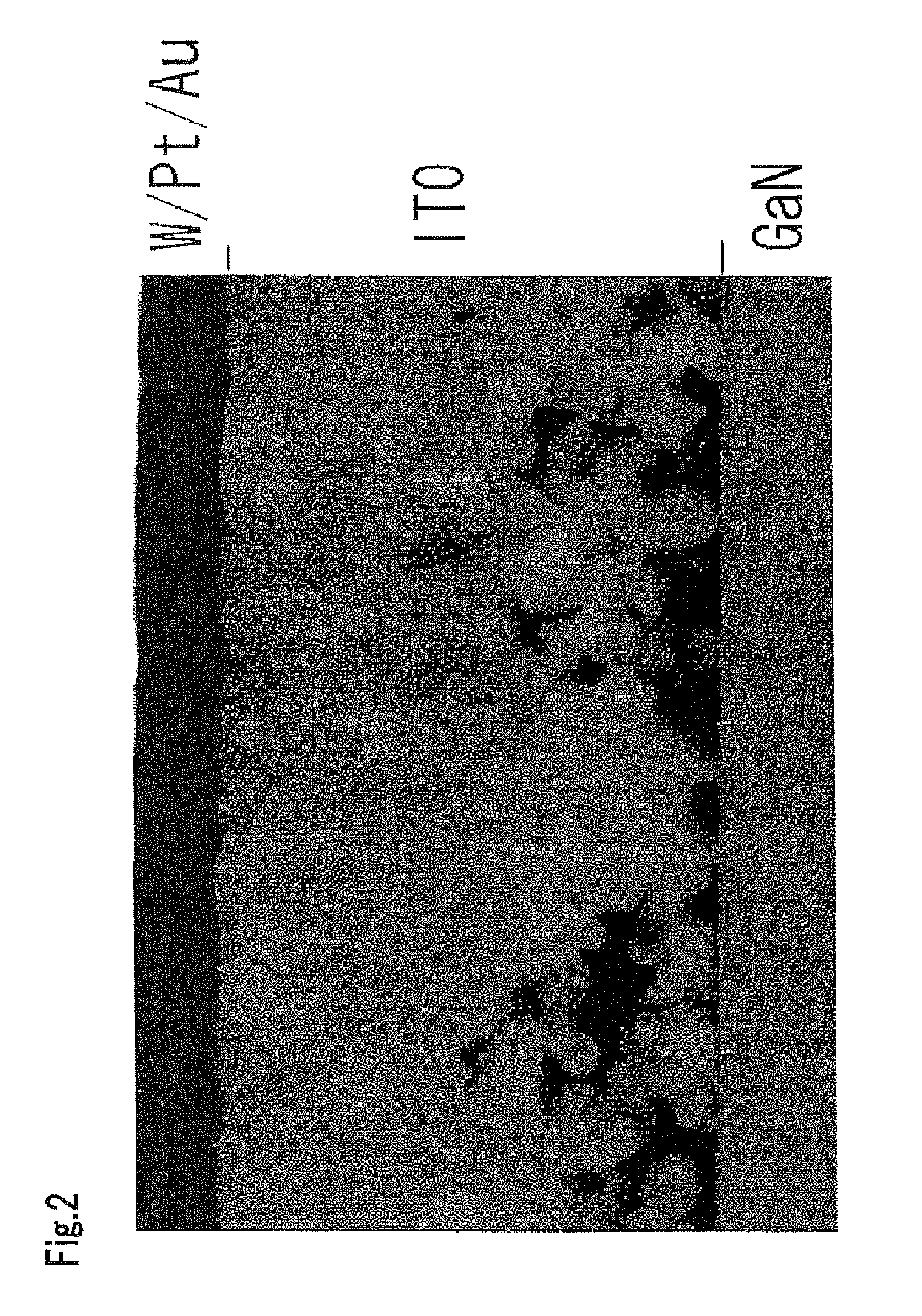
[0147] With the semiconductor light emitting element thus obtaining, like with that of Example 1, the ohmic characteristics are excellent, transmissivity was good, light extraction efficiency will be increased, and the electrode side thereof will...

example 3

[0148] The semiconductor light emitting element of this example has substantially the same construction as that of Example 1, except that after the ITO film is formed in the production method of Example 1, or after a 5000 Å ITO film is formed while maintaining a constant RF power at room temperature in the production method of Example 1, lamp annealing is performed at, for example, 500 to 600° C. in a reducing gas atmosphere (e.g., a hydrogen gas atmosphere).

[0149] With the semiconductor light emitting element thus obtaining, like with that of Example 1, the ohmic characteristics are excellent, transmissivity is good, light extraction efficiency will be increased, and the electrode side thereof will be made into a light emission observation surface.


PUM


Abstract

A semiconductor light emitting element includes an conductive oxide film containing at least one element selected from the group consisting of zinc, indium, tin, and magnesium that is electrically connected to the semiconductor layer. The conductive oxide film includes a plurality of voids in the vicinity of the interface with the semiconductor layer.

Description

BACKGROUND OF THE INVENTION [0001] 1. Field of the Invention [0002] The present invention relates to a semiconductor light emitting element having a transparent conductive oxide film as an electrode. [0003] 2. Background Information [0004] Semiconductor light emitting elements having a p-type semiconductor layer and an n-type semiconductor layer laminated onto a substrate, and electrodes that are electrically connected to the respective p-type and n-type semiconductor layers, are well known in the prior art. In addition, as the electrode that is electrically connected to the p-type semiconductor layer, a structure in which an electrode made of a transparent material is formed on the entire surface of the p-type semiconductor layer and a metal electrode is formed thereon, is well known. [0005] With semiconductor light emitting elements having this type of structure, in order to improve light extraction efficiency, a transparent metal thin film, or a conductive oxide film of ITO, ZnO,...

Claims


Application Information

Patent Timeline
IPC IPC(8): H01L21/00H01L33/38H01L33/42H01L33/48H01L33/62
CPCH01L33/20H01L33/38H01L2924/07802H01L24/45H01L2224/73265H01L2224/48247H01L2224/32245H01L2224/45144H01L2933/0016H01L33/42H01L33/486H01L33/62H01L2924/00H01L2924/00014H01L2924/12032H01L2924/12042H01L2924/181H01L2224/0603H01L2224/48257H01L2924/00012
Inventor DEGUCHI, KOICHIROKASAI, HISASHIKUSUSE, TAKESHIHONJO, KOJIYAMADA, TAKAO
Owner NICHIA CORP
Why Eureka
Try Eureka