Method of forming polymide coating containing dielectric filler on surface of metallic material process for producing copper clad laminate for formation of capacitor layer for printed wiring board and copper clad laminate obtained by the process

a technology of dielectric filler and metallic material, which is applied in the direction of electrophoretic coating, insulating substrate metal adhesion improvement, and semiconductor/solid-state device details, etc., can solve the problems of easy decomposition and unstable of polyamide acid, and achieve the effect of preventing any damage and high strength and flexibility

Inactive Publication Date: 2005-07-28
MITSUI MINING & SMELTING CO LTD
View PDF2 Cites 65 Cited by
  • Summary
  • Abstract
  • Description
  • Claims
  • Application Information

AI Technical Summary

Benefits of technology

[0049] It is indeed possible to manufacture a copper clad laminate by way of using two pieces of the above-described copper foil with a dielectric filler-containing polyimide coating, overlapping each dielectric filler-containing polyimide coating, and pressing them. However, the above method of manufacturing a copper clad laminate made it possible to manufacture a dielectric filler-containing dielectric layer having an optional and uniform thickness, thereby allowing to form an extremely thin dielectric layer. Further, since the dielectric layer of the copper clad laminate according to the present invention is a polyimide coating in which dielectric fillers have been dispersed, it has enough high strength and flexibility which are both features of a polyimide resin, so that the dielectric layer will not be embrittled and prevent any damage caused by a showering of the etching solution conducted at the time of forming a capacitor circuit.

Problems solved by technology

However, polyamide acid is easily decomposable and unstable.

Method used


Image

  • Method of forming polymide coating containing dielectric filler on surface of metallic material process for producing copper clad laminate for formation of capacitor layer for printed wiring board and copper clad laminate obtained by the process
  • Method of forming polymide coating containing dielectric filler on surface of metallic material process for producing copper clad laminate for formation of capacitor layer for printed wiring board and copper clad laminate obtained by the process
  • Method of forming polymide coating containing dielectric filler on surface of metallic material process for producing copper clad laminate for formation of capacitor layer for printed wiring board and copper clad laminate obtained by the process

Examples


example 1

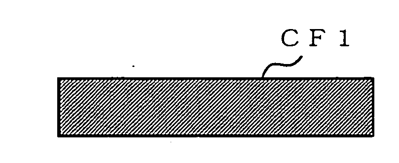
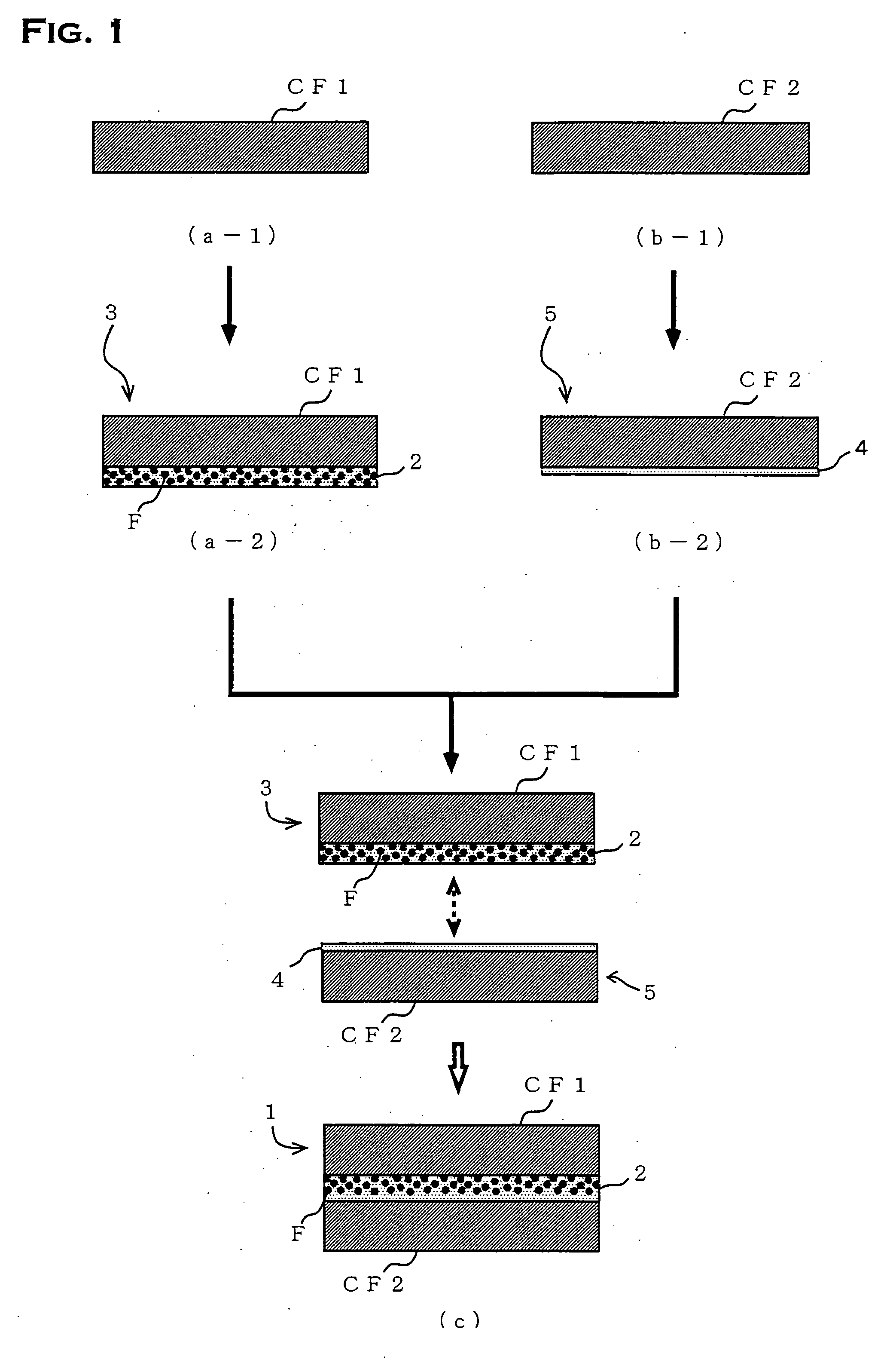
[0054] In the present example, a copper clad laminate 1 for forming a capacitor layer for use in a printed wiring board was manufactured based on a production flow shown in FIG. 1. In the example, a very low profile (VLP) with a nominal thickness of 35 μm was employed as a first copper foil CF1.

[0055] In advance of forming a dielectric filler-containing polyimide coating 2 on a surface of the first copper foil CF1, an acid pickling treatment and electrolytic degreasing treatment were conducted for cleaning the surface of the first copper foil CF1 in a step of (a-1) in FIG. 1. The acid pickling treatment was carried out with the first copper foil CF1 immersed for 1 minute in a sulphuric acid solution having a liquid temperature of 25° C. and concentration of 1M, and then the first copper foil CF1 was rinsed with water.

[0056] Subsequently, an alkaline degreasing aqueous solution containing 20 g / L of sodium carbonate and 5 g / L of trisodium phosphate was employed to degrease for 1 min...

example 2

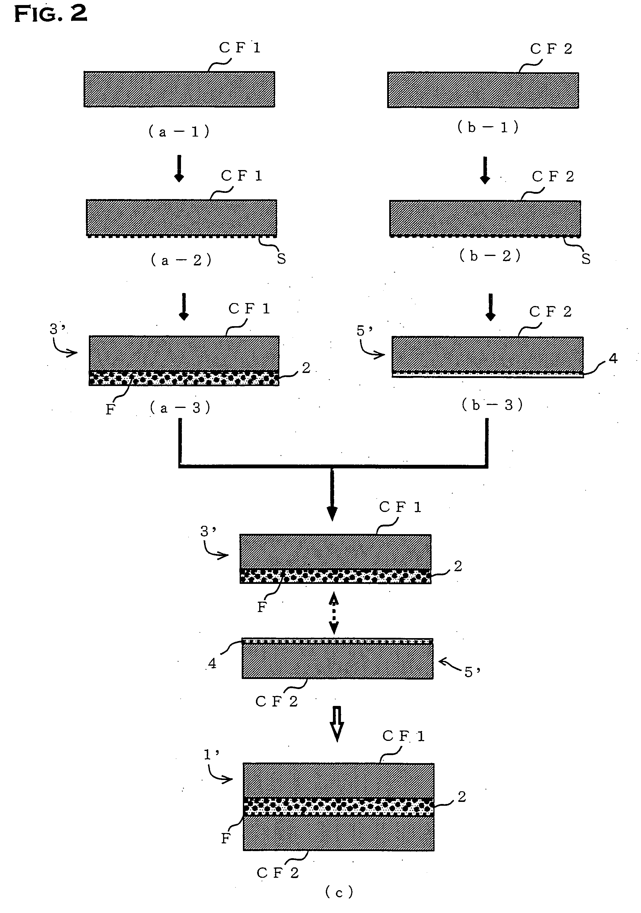
[0066] The present example describes manufacture of a copper clad laminate 1′ for forming a capacitor layer for use in a printed wiring board based on a production flow shown in FIG. 2. In the present example, a very low profile (VLP) with a nominal thickness of 35 μm was employed as a first copper foil CF1, as in the case of Example 1.

[0067] The steps carried out at the stage in FIG. 2(a-1) which include acid pickling and degreasing treatments are the same as those done in Example 1. On completion of a degreasing treatment, a nickel metallic seed layer S as shown in FIG. 2(a-2) was provided, and then a dielectric filler-containing polyimide coating 2 was formed on the surface of the first copper foil CF1 as shown in FIG. 2(a-3) to prepare a copper foil 3 with a dielectric filler-containing polyimide coating. As to formation steps for a dielectric filler-containing polyimide coating 2 after provision of a metallic seed layer S are the same as done in Example 1.

[0068] Therefore, on...


PUM

PropertyMeasurementUnit
particle size DIAaaaaaaaaaa
particle sizeaaaaaaaaaa

Abstract

A method of forming a dielectric layer containing dielectric filler, which is excellent in film thickness uniformity, from a polyimide electrodeposition liquid containing dielectric filler. In particular, a method of forming a polyimide coating container dielectric filler on a surface of metallic material according to the electrodeposition coating technique, characterized in that as the dielectric filler, use is made of dielectric powder of perovskite structure in approximately spherical form which has an average particle diameter (D1A) of 0.05 to 1.0 μm and a weight cumulative particle diameter (D50), measured in accordance with the laser diffraction scattering type particle size distribution measuring method, of 0.1 to 2.0 μm and further exhibits an aggregation degree, in terms of D50/D1a wherein D50 and D1a represent a weight cumulative particle diameter and an average particle diameter obtained by image analysis, respectively, of 4.5 or less.

Description

TECHNICAL FIELD [0001] The present invention relates to a method of forming a dielectric filler-containing polyimide coating on a metallic material such as copper, method of manufacturing a copper clad laminate for forming a capacitor layer for use in a printed wiring board, and copper clad laminate obtained through the manufacturing method. BACKGROUND ART [0002] In these years, it has become general practice that a capacitor structure is formed by using a copper clad laminate in a printed wiring board, in particular, in the internal layer portion of a multilayer printed wiring board, in a manner similar to that in circuit shape formation, and the capacitor structure thus formed is utilized as a built-in capacitor. The formation of a capacitor structure in the internal layer portion of a multilayer printed wiring board has permitted omitting the capacitors arranged on the external layer surface, and hence the miniaturization and high densification of the external layer circuits has ...

Claims


Application Information

Patent Timeline
Patent Type & Authority Applications(United States)
IPC IPC(8): C25D7/00C25D13/06C25D15/00C25D15/02H01L23/12H05K1/16H05K3/38
CPCC25D15/02H05K1/162H05K3/384H05K2201/0154H05K2203/135H05K2201/0355H05K2201/09309H05K2203/0723H05K2201/0209
Inventor YOKOTA, TOSHIKOTAKAHASHI, SUSUMUMATSUSHIMA, HIDEAKIDOBASHI, MAKOTOYAMAMOTO, TAKUYA
Owner MITSUI MINING & SMELTING CO LTD
Why Eureka
Try Eureka