Flash memory devices using large electron affinity material for charge trapping

a technology of electron affinity and charge trapping, which is applied in the field of field effect transistors, can solve the problems of difficult scaling down of dram cells, limited data retention capability of dram, and frequent refreshing of dram with attendant power consumption, and achieves high permittivity

Inactive Publication Date: 2005-08-04
RGT UNIV OF CALIFORNIA
View PDF2 Cites 52 Cited by
  • Summary
  • Abstract
  • Description
  • Claims
  • Application Information

AI Technical Summary

Benefits of technology

[0009] In accordance with the invention, a gate-stack structure is provided for a flash memory device which includes a tunnel dielectric layer on a surface of a semiconductor body over a channel region of the device. An electron-trapping dielectric layer

Problems solved by technology

It is difficult to scale down the DRAM cell size due to need for a sizable cell capacitance, however.
The data retention capability of DRAM is limited by charge leakage through p-n junctions and sub-threshold conduction in transistors; therefore DRAM needs frequent refreshing with attendant power consumption.
This thickness makes the cell relatively slow to p

Method used


Image

  • Flash memory devices using large electron affinity material for charge trapping
  • Flash memory devices using large electron affinity material for charge trapping
  • Flash memory devices using large electron affinity material for charge trapping

Examples


Embodiment Construction

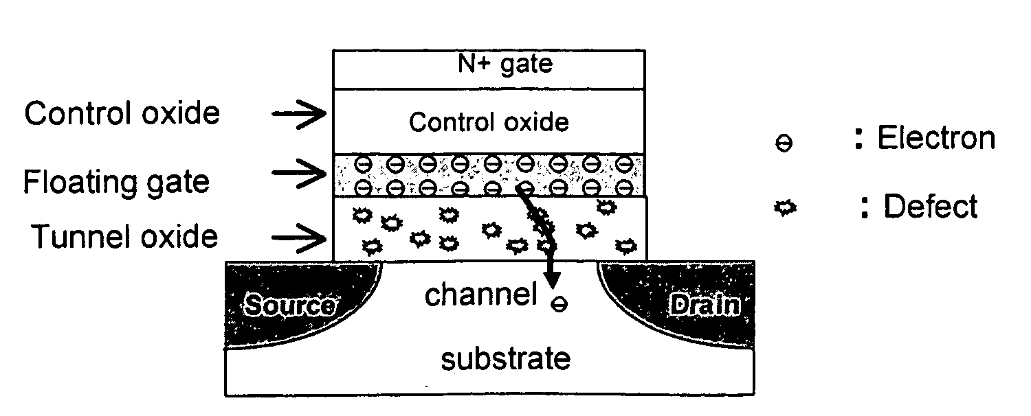
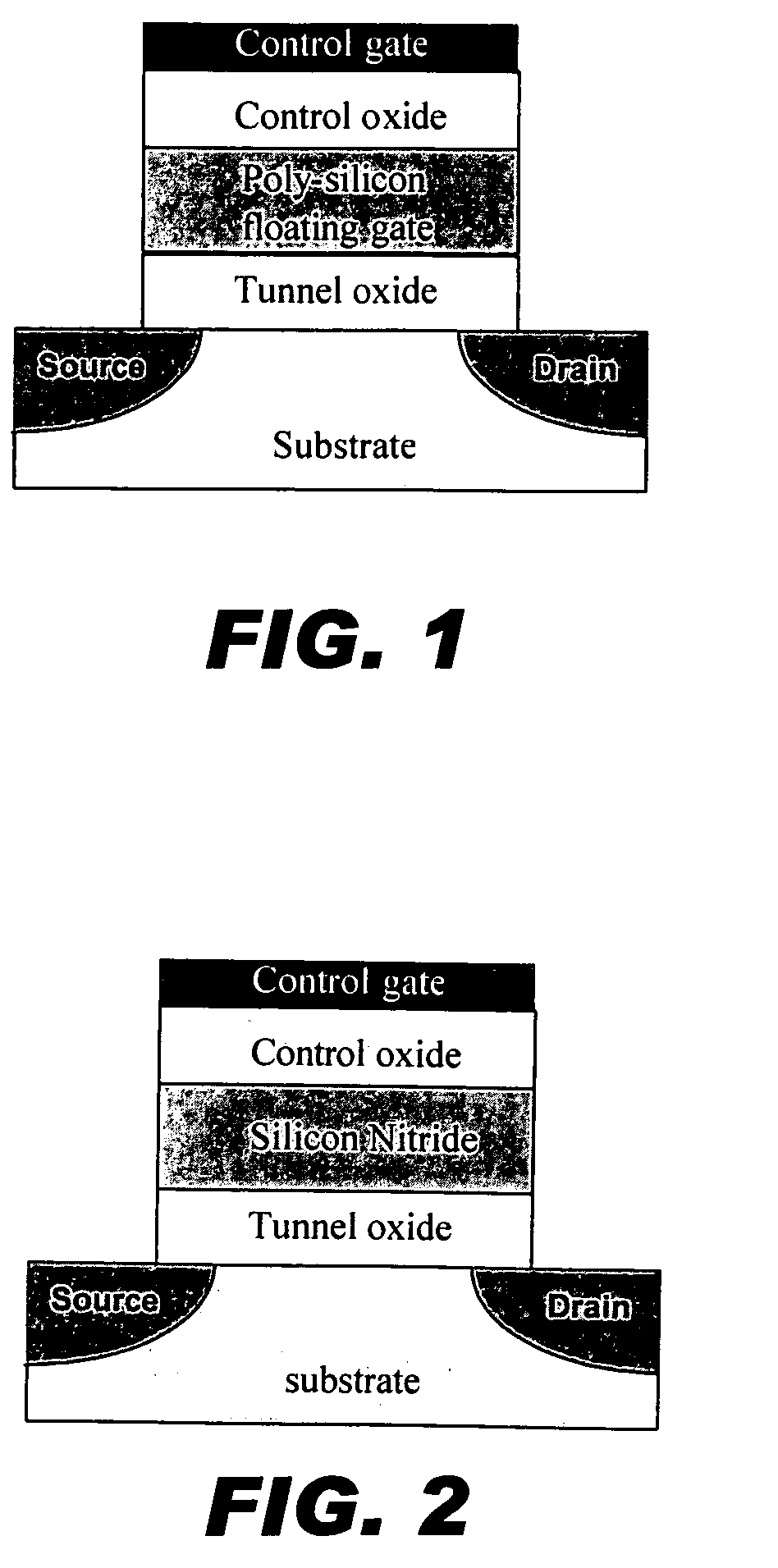
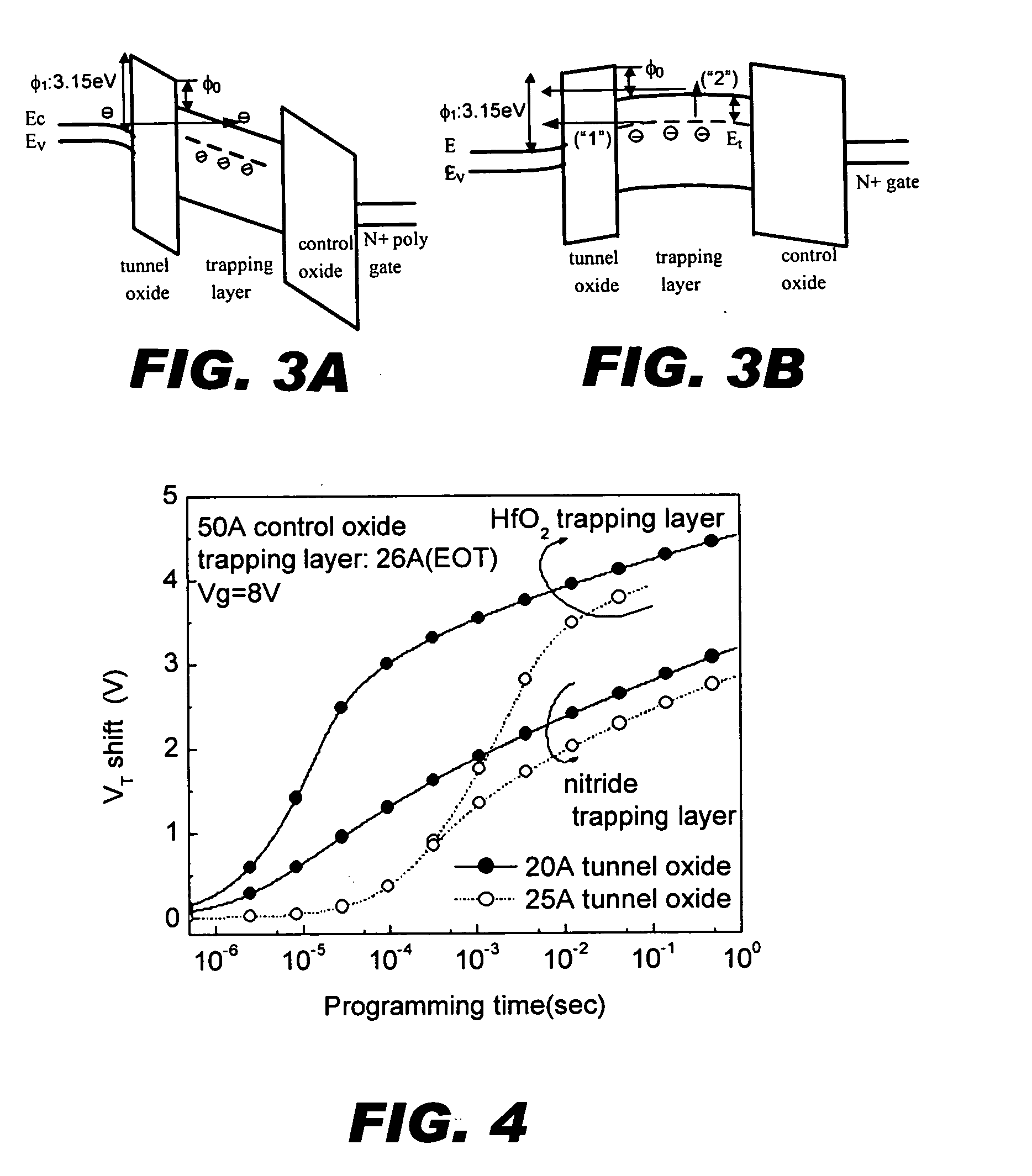
[0023] In order to improve the programming speed and / or lower the programming voltage of a SONOS-type memory device, it is desirable to use an electron-trapping material with a lower conduction band edge (higher electron affinity) to achieve a larger offset φ0, as well as to provide for programming by direct tunneling at low voltages. In accordance with the invention, a high-permittivity (“high-k”) dielectric material such as HfO2 or ZrO2 replace silicon nitride as the electron trapping material. Such materials have a lower conduction band edge than does silicon nitride. A comparison of dielectric material properties is given in Table 3. If HfO2 were to be used as the trapping layer, φ0 would be 1.65 eV, which is much better than the 1.03 eV barrier associated with a nitride-trapping layer. Thus, it is advantageous to use a high-k material as the trapping layer in a SONOS-type memory device, provided that it contains a sufficient density of deep trap states. In principle, the trap d...


PUM


Abstract

Disclosed is a novel flash memory device using a high-permittivity dielectric such as HfO2 or TiO2 as a charge trapping layer. Numerical simulation shows that the novel trapping material will enhance the retention time/programming speed ratio by 5 orders of magnitude, compared to the conventional Si3N4 trapping layer. Capacitors with HfO2 deposited by RTCVD as the charge trap/storage layer in SONOS-type flash memory devices were fabricated and characterized. Compared against devices with Si3N4 trapping layer, faster programming speed as well as good retention time is achieved with low programming voltage.

Description

CROSS REFERENCE TO RELATED APPLICATIONS [0001] This application claims priority under 35 USC 120 from Provisional patent application Ser. No. 60 / 537,928, filed Jan. 20, 2004 which is incorporated herein by reference for all purposes.BACKGROUND OF THE INVENTION [0002] This invention relates generally to semiconductor memory devices, and more particularly the invention relates to field effect transistors having a charge storage layer between a channel region and a control gate for programming the threshold voltage for current conduction in the channel. [0003] Memory is a key component of any electronic system such as a personal computer, cellular phone, digital camera, network router, handheld personal digital assistant, etc. Demand for increased memory capacity and lower cost drives the miniaturization of semiconductor memory cells and also dictates low-power cell designs for use in future portable electronic systems. [0004] There are mainly three kinds of semiconductor memory in the...

Claims


Application Information

Patent Timeline
IPC IPC(8): H01L21/28H01L29/51H01L29/792
CPCH01L21/28194H01L21/28202H01L29/792H01L29/517H01L29/518H01L29/511
Inventor SHE, MINKING, TSU-JAE
Owner RGT UNIV OF CALIFORNIA
Why Eureka
Try Eureka