Organic light-emitting display device
a light-emitting display and organic technology, applied in the direction of discharge tube luminescnet screens, identification means, instruments, etc., can solve the problems of shortened life of the oled, slow response of the lcd, narrow viewing angle compared to the crt display, etc., to improve the efficiency of electron injection
- Summary
- Abstract
- Description
- Claims
- Application Information
AI Technical Summary
Benefits of technology
Problems solved by technology
Method used
Image
Examples
embodiment 1
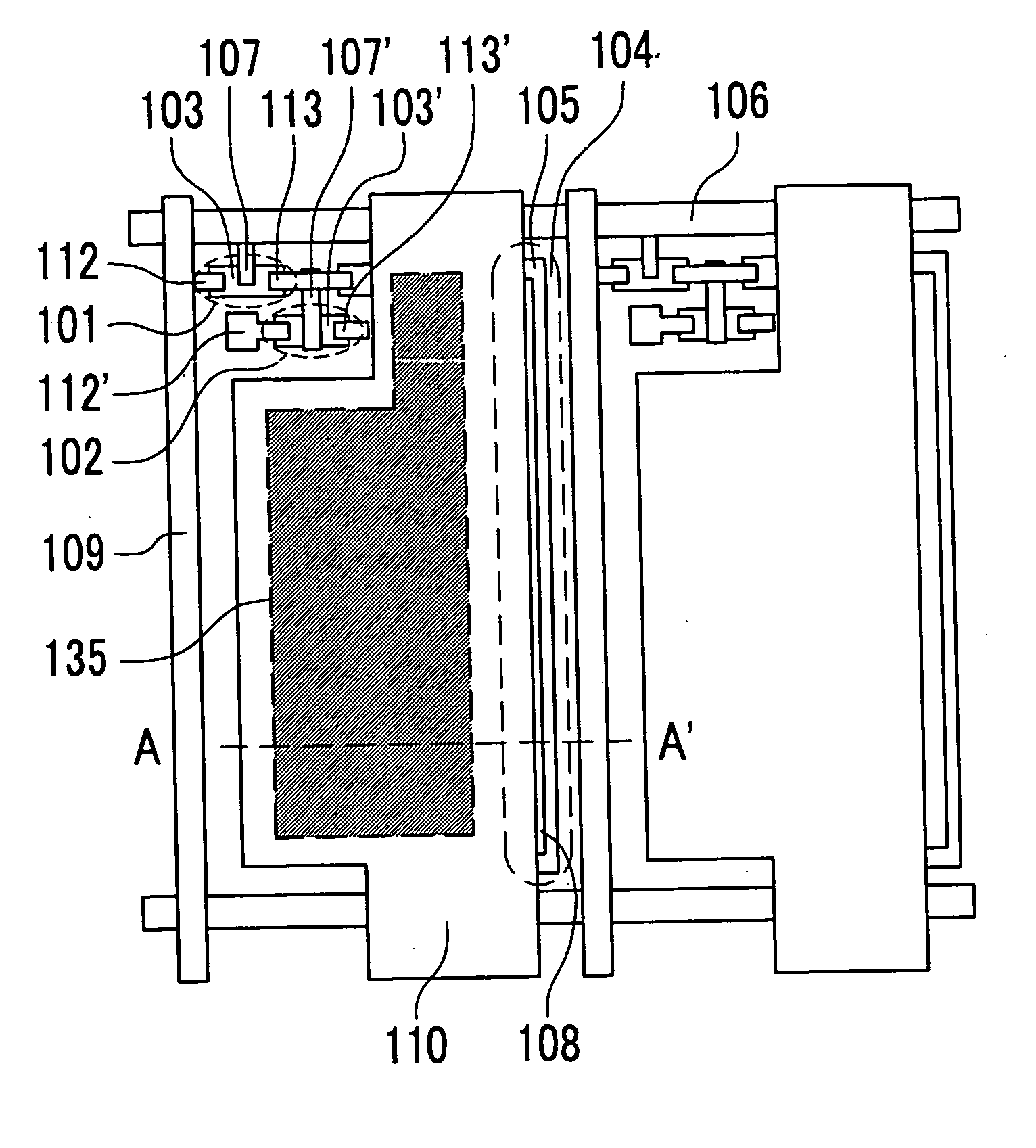
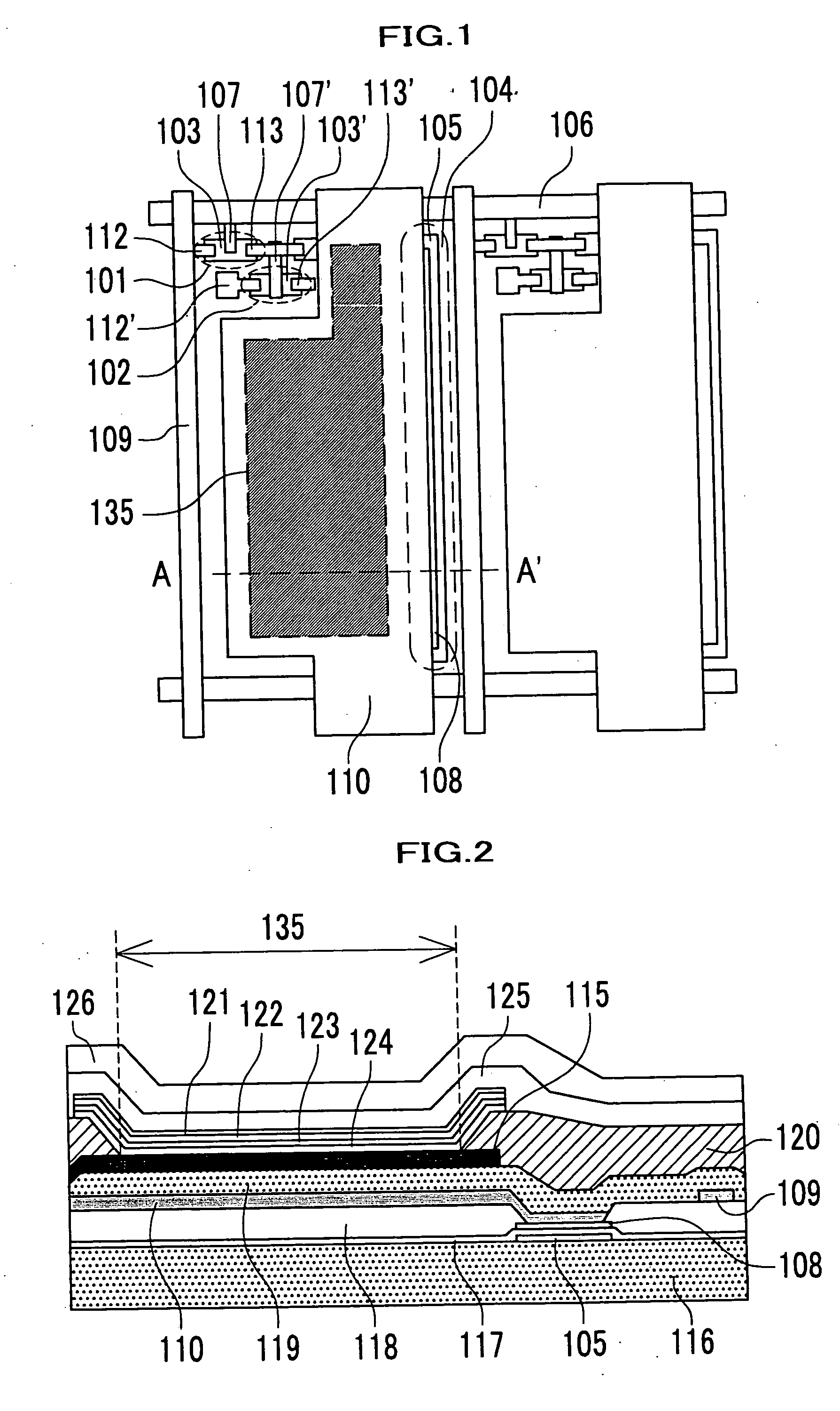
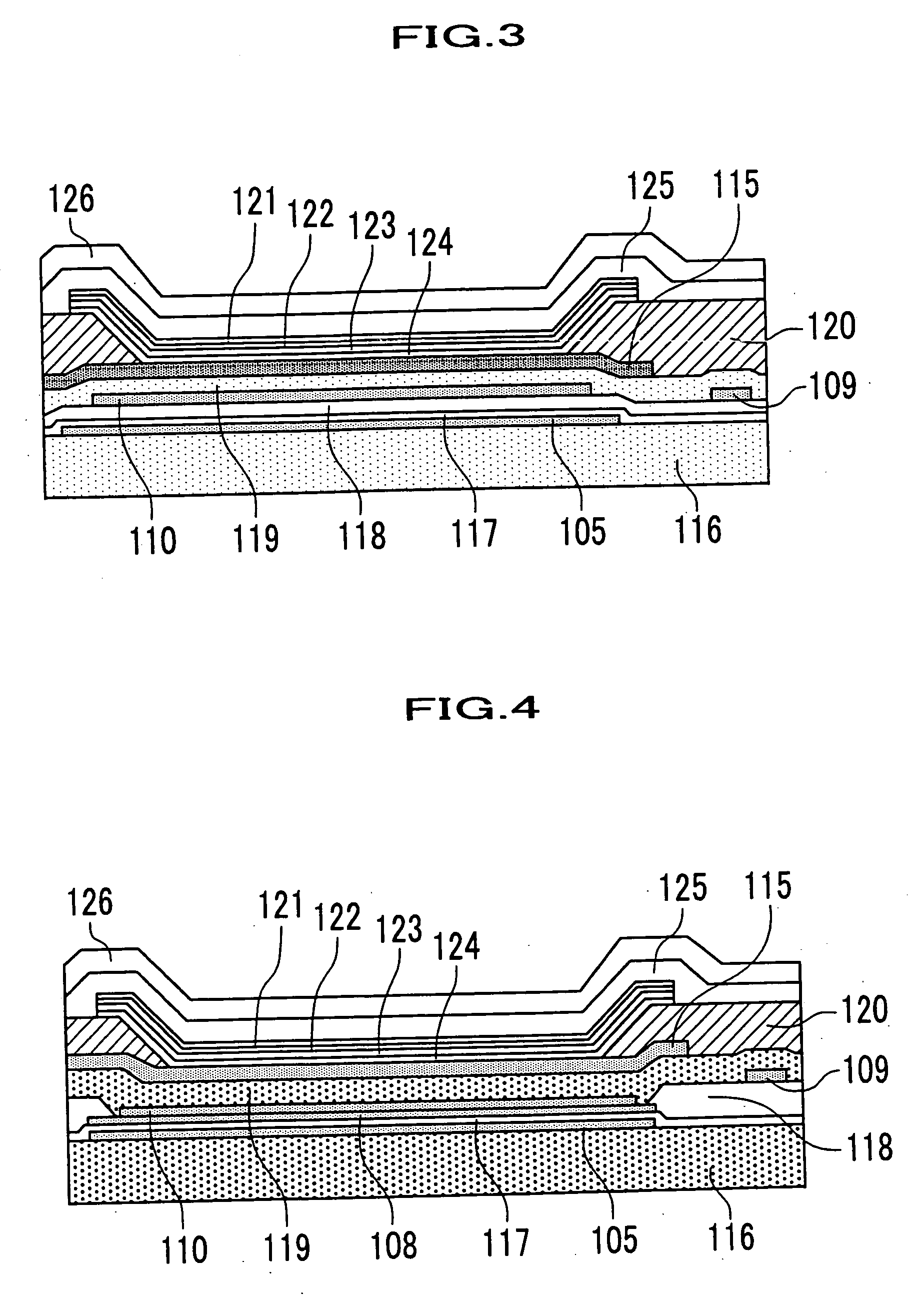
[0050]FIG. 1 is a plan view of a configuration of an OLED according to the embodiment 1 of the present invention. FIG. 2 is a sectional view of the light-emitting element taken along line A-A′ of FIG. 1. The OLED shown in FIGS. 1 and 2 comprises plural light-emitting elements, each of which is arranged in a matrix and has an organic light-emitting element. The organic light-emitting element consists of an organic light-emitting layer 122 and an upper electrode 125 and a lower electrode 115 sandwiching the organic light-emitting layer 122. This organic light-emitting element is the type of the top emission where light is emitted from the organic light-emitting layer 122 and then the light is taken out from the upper electrode 125. Reference numerals 121, 123, 124 and 126 denote a hole transport layer, an electron transport layer, an electron injection layer and an protective layer, respectively.
[0051] In FIG. 1, reference numeral 101 denotes a 1st TFT. Reference numerals 112, 113, 1...
embodiment 2
[0067] Now, an OLED using an upper electrode as a cathode will be explained below. FIG. 5 shows a cross cut section of the region including a light-emitting element in OLED taken along line A-A′ of FIG. 1, according to the embodiment 2 of the present invention. The OLED of the embodiment 2 comprises an upper electrode 125 as a cathode and a lower electrode 115 as an anode, which is different from the structure of the previous embodiment 1. Hereinafter, the manufacturing method in the embodiment 2 will be explained.
[0068] First, amorphous silicon (a-Si) with film thickness 50 nm is formed on a glass substrate 116 using LPCVD (Low Pressure CVD). Then the total area of the a-Si is laser-annealed and the a-Si is crystallized to form a poly-crystalline Si (p-Si). Next, by patterning the p-Si using a dry etching, an active layer 103 for a 1st transistor 101, an active layer 103′ for a 2nd transistor 102 and a lower capacitor electrode 105 are formed.
[0069] After that, a gate insulating ...
embodiment 3
[0082]FIG. 6 is a plan view of the substantial part in an OLED according to the embodiment 3 of the present invention. TFTs of inverted-stagger structure are applied to this embodiment 3, where a 1st TFT 101 and a 2nd TFT are formed by the inverted-stagger structures, dissimilar to the previous embodiments 1 and 2. The reference numerals in the FIG. 6 denote the same meanings as those shown in FIG. 1. Hereinafter, a manufacturing method of the OLED according to the embodiment 3 will be explained.
[0083] First, a gate electrode 107 of the 1st TFT 101 and a gate electrode 107′ of the 2nd TFT 102 are formed using TiW with thickness 50 nm by a sputtering and then patterned with prescribed patterns. Simultaneously to this process, a scan line 106 and a lower capacitor electrode 105 are patterned. Next, a gate insulating film 117 of SiO2 with thickness 100 nm is formed. The SiO2 film is formed by a plasma enhanced CVD (PECVD) using tetraethoxysilane as a source.
[0084] Next, a film of amo...
PUM
 Abstract
Description
Claims
Application Information


