Top-emitting nitride-based light-emitting device and method of manufacturing the same

a technology of topemitting nitride and light-emitting device, which is applied in the direction of solid-state devices, electric lighting sources, and light sources. it can solve the problems of high light reflectivity, low work function, and inability to meet the requirements of large-area, high-brightness light-emitting device, etc., and achieve low specific ohmic contact resistance, low light transmittance, and low work function

Active Publication Date: 2005-09-15
SAMSUNG ELECTRONICS CO LTD +1
View PDF13 Cites 49 Cited by
  • Summary
  • Abstract
  • Description
  • Claims
  • Application Information

AI Technical Summary

Benefits of technology

[0024] Embodiments of the present invention provide a top-emitting nitride-based light-emitting device having a transparent ohmic contact electrode structure with high light transmittance, low sheet resistance, and low specific ohmic contact resistivity and a method of manufacturing the same.

Problems solved by technology

However, using only TCO or TCN film as a p-type transparent ohmic electrode for a top-emitting gallium nitride (GaN)-based light-emitting device may cause many problems since the TCO or TCN film exhibits high sheet resistance, high light reflectivity, and low work function under conditions for film formation.
The first problem is that the above-enumerated transparent conducting thin films are not suitable for use in large-area, large-capacity, and high-brightness light-emitting devices because their high sheet resistance of approximately 100 Ω / cm2 will hinder current spreading along a lateral direction (parallel to interlayer between layers) and vertical hole injection during film formation using physical vapor deposition (PVD) such as sputtering, electron-beam (e-beam) or heat evaporation, or pulsed laser deposition (PLD).
The second problem is that a p-GaN surface being exposed to plasma ions when the transparent conducting film is deposited using plasma can be easily damaged, thus degrading electrical characteristics.
The third problem is that the luminous efficiency of the transparent conducting film decreases due to its high reflectivity with respect to light emitted by a GaN-based light-emitting device.
The last problem is that when a TCO is used as an electrode in direct ohmic contact with a GaN-based compound semiconductor, insulating gallium oxide (Ga2O3) and magnesium oxide (MgO) are formed on the GaN surface during deposition of the thin film on the GaN due to the strong oxidizing power of Ga and Mg (a p-type dopant), thereby making it difficult to achieve a high quality ohmic contact electrode.
However, due to their low luminous efficiency, TLEDs using a semi-transparent Ni / Au ohmic contact layer suffer the limitation of not being able to realize the next generation light-emitting devices with large capacity and high brightness.
However, the FCLED also suffers from problems such as high resistance due to poor adhesion and oxidation of the reflective layer.
However, the proposed method is not suitable for use in high volume applications because of high specific contact resistivity and addition of the step of oxidizing the Ni / Au (or Ag).
As described above, there are the following fundamental problems that make it difficult to develop a high quality ohmic contact electrode.
Second, a SBH is increased at the interface between a p-GaN and an electrode due to the absence of a transparent electrode material having a work function higher than the p-GaN, thereby hindering vertical hole injection.
Fifth, the surface of a p-GaN can be easily damaged by plasma during sputtering that allows for formation of a transparent conducting layer with a low sheet resistance.
Due to the above-mentioned problems, the amount of heat generated between the p-GaN and the ohmic contact layer increases, thus decreasing the life span and reliability of a light-emitting device.

Method used


Image

  • Top-emitting nitride-based light-emitting device and method of manufacturing the same
  • Top-emitting nitride-based light-emitting device and method of manufacturing the same
  • Top-emitting nitride-based light-emitting device and method of manufacturing the same

Examples


first embodiment

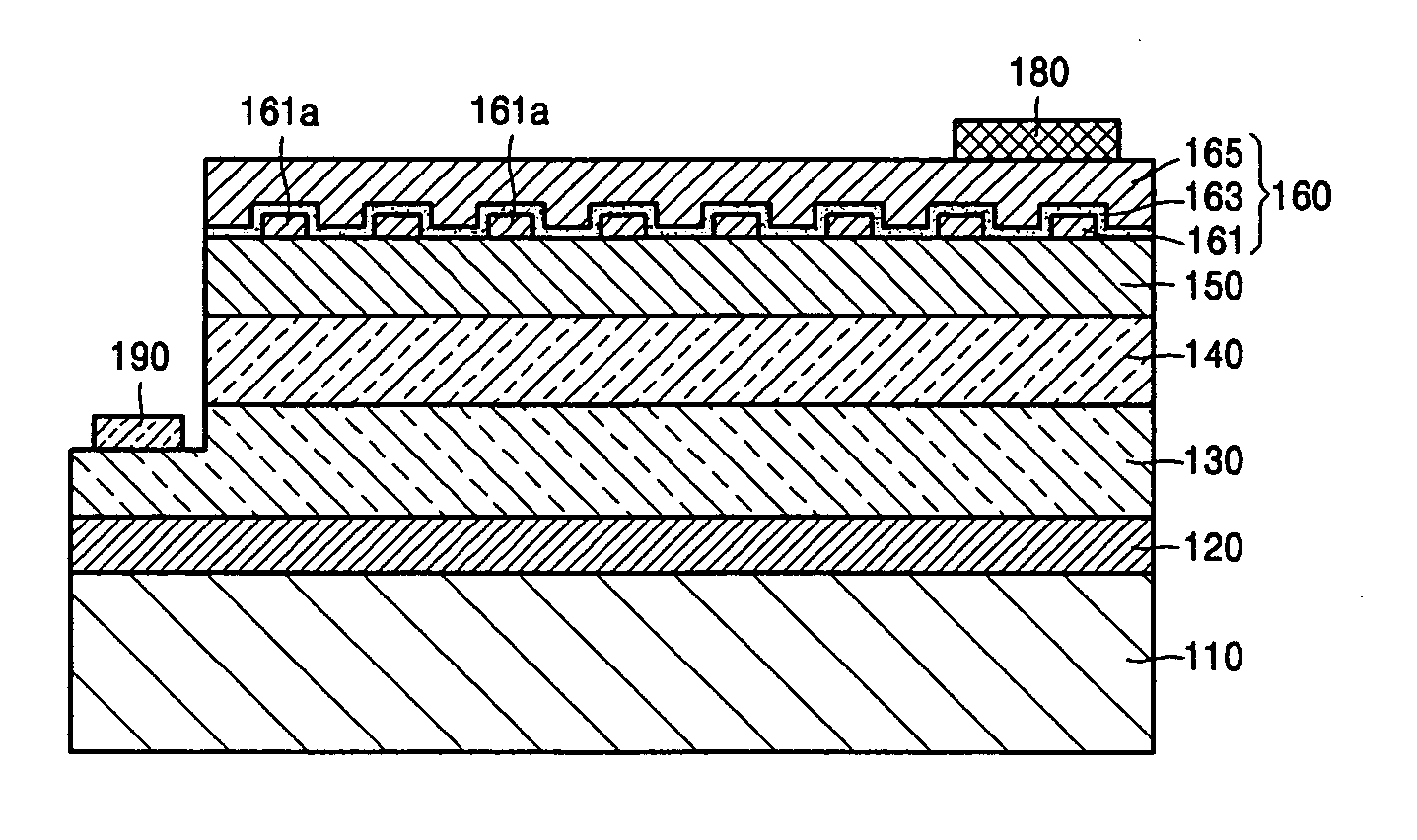
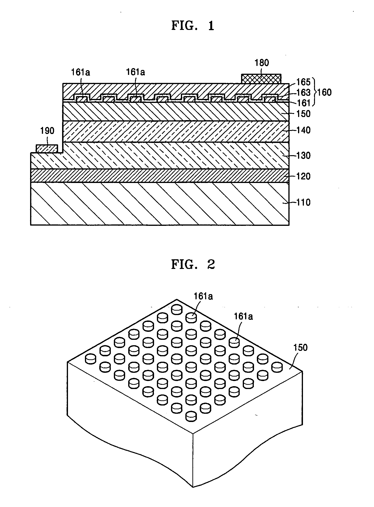
[0038] Referring to FIG. 1, a top-emitting light-emitting device according to the present invention includes a substrate 110, and a buffer layer 120, an n-cladding layer 130, an active layer 140, a p-cladding layer 150 and a transparent multilayer ohmic contact 160 sequentially formed on the substrate 110. The top-emitting light-emitting device further includes a p-electrode pad 180 and an n-electrode pad 190.

[0039] The top-emitting light-emitting device is mainly divided into a light-emitting structure including the substrate 110, the buffer layer 120, the n-cladding layer 130, the active layer 140, and the p-cladding layer 150 and a p-electrode structure including the transparent multilayer ohmic contact 160 formed on the p-cladding layer 150. The substrate 110 may be formed from sapphire, silicon carbide (SiC), Si, or gallium arsenide (GaAs). Optionally, the buffer layer 120 may not be formed.

[0040] Each of the layers from the buffer layer 120 up to the p-cladding layer 150 incl...

second embodiment

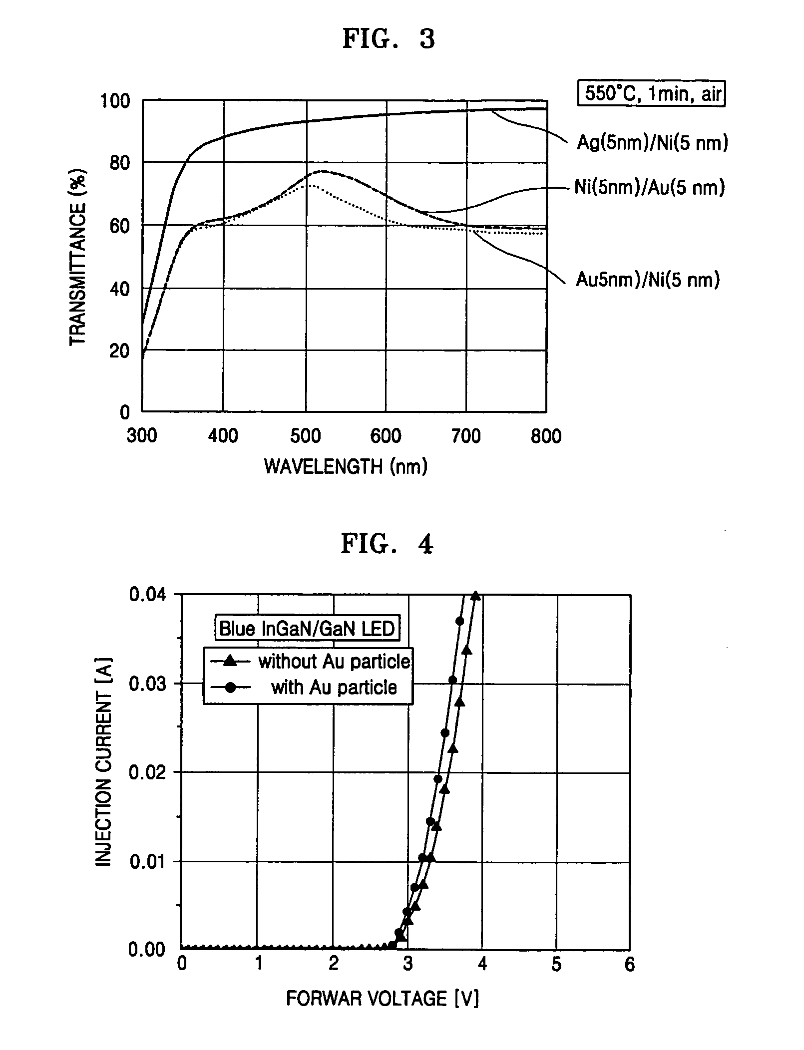
[0055] A curve with dash marks on the graph represents light transmittance obtained by annealing a light-emitting device with a p-electrode structure according to the present invention at 530° C. The p-electrode structure comprises the grid cell layer 161 composed of a regular grid array of Au particles with a size of 20 μm on the p-cladding layer 150, the surface protective layer 163 formed by sequentially depositing Ni (5 nm) and Au (5 nm), and the transparent conducting layer 165 made of ITO with a thickness of 100 nm.

[0056] A curve with dot marks represents light transmittance obtained by annealing a light-emitting device with a conventional p-electrode structure formed by sequentially depositing Au (5 nm) and Ni (5 nm) on the p-cladding layer 150 at 530° C.

[0057] As evident from FIG. 3, the light-emitting devices according to the present invention exhibit improved light transmittances over the conventional light-emitting device. Furthermore, the light-emitting devices accordin...


PUM


Abstract

A top-emitting nitride-based light-emitting device and a method of manufacturing the same. The top-emitting nitride-based light-emitting device having a substrate, an n-cladding layer, an active layer, and a p-cladding layer sequentially formed includes: a grid cell layer formed on the p-cladding layer by a grid array of separated cells formed from a conducting material with a width of less than 30 micrometers to improve electrical and optical characteristics; a surface protective layer that is formed on the p-cladding layer and covers at least regions between the cells to protect a surface of the p-cladding layer; and a transparent conducting layer formed on the surface protective layer and the grid cell layer using a transparent conducting material. The light-emitting device and the method of manufacturing the same provide an improved ohmic contact to the p-cladding layer, excellent I-V characteristics, and high light transmittance, thus increasing luminous efficiency of the device.

Description

CROSS-REFERENCE TO RELATED PATENT APPLICATION [0001] This application claims the benefit of Korean Patent Application No. 10-2004-0016271, filed on Mar. 10, 2004, in the Korean Intellectual Property Office, the disclosure of which is incorporated herein in its entirety by reference. BACKGROUND OF THE INVENTION [0002] 1. Field of the Invention [0003] Embodiments of the present invention relate to a top-emitting nitride-based light-emitting device, and a method of manufacturing the same, and more particularly, to a top-emitting nitride-based light-emitting device with improved ohmic characteristics and luminous efficiency and a method of manufacturing the same. [0004] 2. Description of the Related Art [0005] Transparent conducting thin films are used for a wide variety of applications in optoelectronics, display, and energy industries. In the field of light-emitting devices, research is being actively conducted around the world to develop a transparent conducting ohmic electrode struc...

Claims


Application Information

Patent Timeline
Patent Type & Authority Applications(United States)
IPC IPC(8): H01L21/00H01L27/15H01L33/06H01L33/32H01L33/38H01L33/42H05B33/26
CPCH01L33/387H01L2933/0016H01L33/42H05B33/26
Inventor SEONG, TAE-YEONKIM, KYOUNG-KOOKSONG, JUNE-OLEEM, DONG-SEOKSOHN, JUNG-INN
Owner SAMSUNG ELECTRONICS CO LTD
Why Eureka
Try Eureka