Scalable self-aligned dual floating gate memory cell array and methods of forming the array

Inactive Publication Date: 2005-09-15
SANDISK TECH LLC
View PDF58 Cites 17 Cited by
  • Summary
  • Abstract
  • Description
  • Claims
  • Application Information

AI Technical Summary

Benefits of technology

[0010] According to one aspect of the present invention, a memory array is made by forming a thin layer of dielectric on the substrate surface and then depositing over it a layer of material that is later separated into conductive floating gates. This dielectric layer, which is preferably a grown oxide, remains as the memory cell floating gate dielectric, and is of high quality because of being formed over a virgin substrate surface. This improves the memory erasure operation when the floating gates are erased to the substrate. The floating gate material is preferably doped polysilicon. Continuous source a

Problems solved by technology

It is often difficult to perform both of these functions in an optimum manner with a single voltage.
But there are usually limits of how far a given circuit layout can be shr

Method used


Image

  • Scalable self-aligned dual floating gate memory cell array and methods of forming the array
  • Scalable self-aligned dual floating gate memory cell array and methods of forming the array
  • Scalable self-aligned dual floating gate memory cell array and methods of forming the array

Examples


first processing example

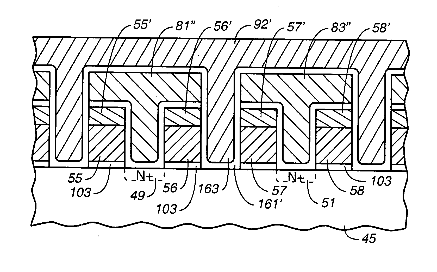
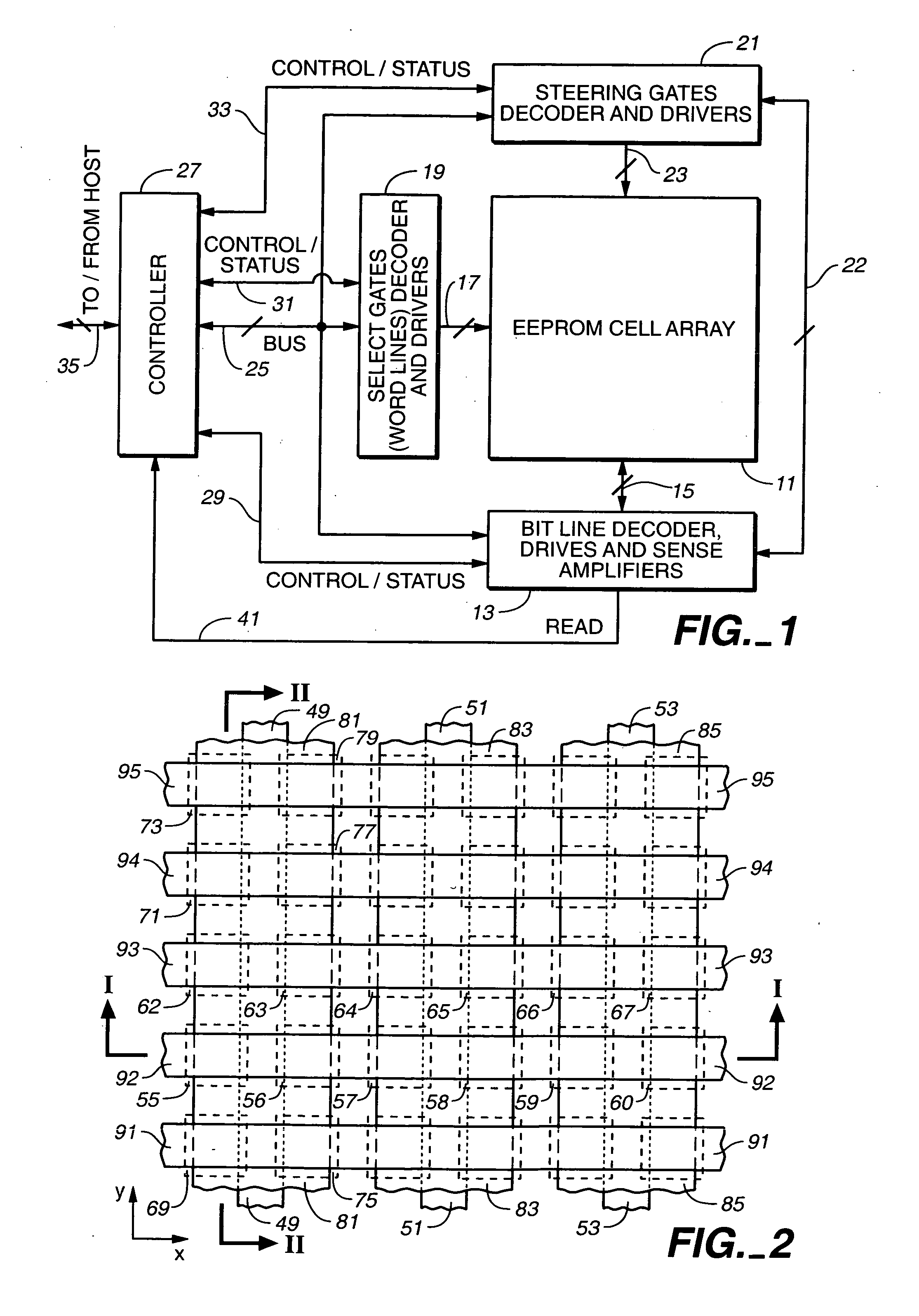
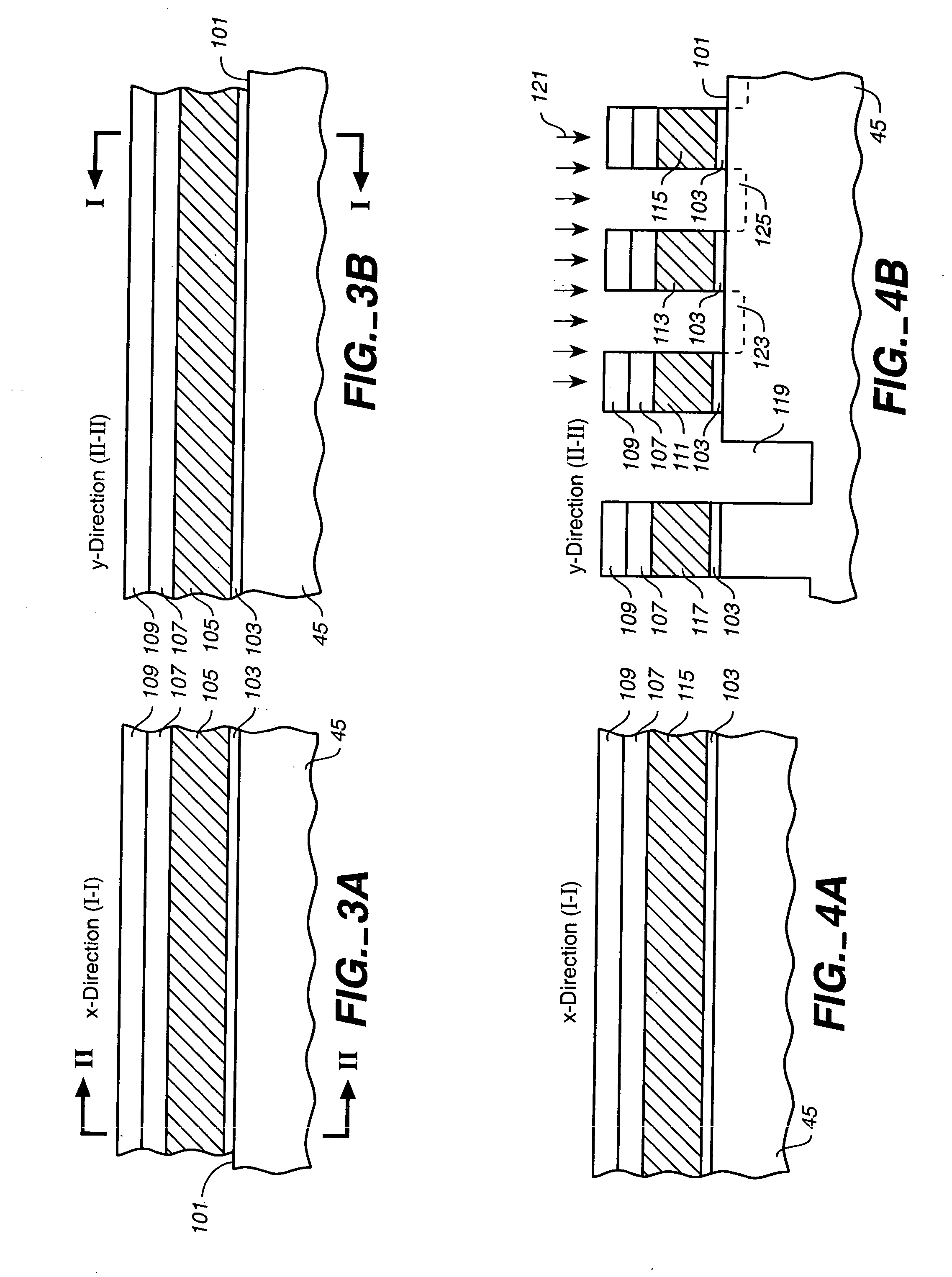
[0051]FIGS. 3-9 illustrate a sequence of steps utilized according to one aspect of the present invention to form the array of FIG. 2, by showing sectional views of FIG. 2 across sections I-I (part A of each figure) and section II-II (part B of each figure). Referring initially to FIGS. 3A and 3B, the result of several initial steps in the semiconductor processing are illustrated. A thin (such as 80-100 Angstroms thick) layer 103 of oxide dielectric is grown over the entire surface 101 of the silicon substrate 45. Next, a thick (such as 500-3000 Angstroms) layer 105 of polysilicon is deposited over the dielectric layer 103. The thickness of the layer 105 is made to be sufficient to provide an amount of coupling along its sidewalls with later formed steering gates that is desired. This polysilicon may be deposited in a doped form or deposited undoped and then doped in a later step by ion implantation. A dielectric layer is then formed over the polysilicon, shown to be two layers. A la...

second processing example

[0069]FIGS. 16-22 show exemplary sequential cross-sectional views of an integrated circuit structure that illustrate many steps of its formation by a process that corresponds to, but differs in certain respects from, the process described above with respect to FIGS. 3-9. The process illustrated in FIGS. 16-22 includes use of narrow source and drain implants (formed differently in FIG. 10), thickened dielectric layers between the substrate and the select gates (described with respect to FIG. 11), “T” shaped floating gates (as shown generally by FIG. 13B) and a double dielectric layer between the select gates and the word lines for a reduced coupling between them. The reference numbers used in FIGS. 16-22 for corresponding elements in FIGS. 3-9 are those of FIGS. 3-9 with 200 added. For example, the semiconductor substrate in FIGS. 16-22 is labeled “245” while the substrate in FIGS. 3-9 is labeled “45”.

[0070]FIGS. 16-19 illustrate some of the preliminary processing steps of this seco...

third processing example

[0087] Yet another method of forming the same type of array as described above is illustrated in FIGS. 23-26, wherein the “A” portion of each figure is a section of a small portion of the memory cell array being formed, taken at section I-I of FIG. 2 (along the x-axis), and the “B” portion of each figure is a section taken at section II-II of FIG. 2 (along the- y-axis). The primary difference between this embodiment and those of the examples described above is that the separation of the first polysilicon strips in the x-direction into individual floating gates occurs during a single masking step, rather than using the nitride reference elements (131, 133, 135 etc. of FIGS. 7 and 8, and 331, 333, 335 of FIGS. 20 and 21) to form masks that are aligned during first and second etching steps. After this single etch has occurred, intermediate polysilicon is formed in each of the spaces between floating gates in the x-direction, this intermediate polysilicon becoming part of the steering g...


PUM


Abstract

An integrated non-volatile memory circuit is formed by first growing a thin dielectric layer on a semiconductor substrate surface, followed by depositing a layer of conductive material such as doped polysilicon on this dielectric layer, the conductive material then being separated into rows and columns of individual floating gates. Cell source and drain diffusions in the substrate are continuously-elongated across the rows. Field dielectric deposited between the rows of floating gates provides electrical isolation between the rows. Shallow trenches may be included between rows without interrupting the conductivity of the diffusions along their lengths. A deep dielectric filled trench is formed in the substrate between the array and peripheral circuits as electrical isolation. Various techniques are included that increase the field coupling area between the floating gates and a control gate. Other techniques increase the thickness of dielectric between control gates in order to decrease the field coupling between them.

Description

CROSS-REFERENCE TO RELATED PATENTS AND APPLICATION [0001] This application is related to U.S. Pat. Nos. 6,103,573 and 6,151,248, and application Ser. No. 09 / 667,344, filed Sep. 22, 2000, which patents and application are expressly incorporated herein in their entirety by this reference.FIELD OF THE INVENTION [0002] This invention relates generally to non-volatile flash memory systems, and, more specifically, to the process of forming memory arrays of memory cells that individually contain two floating gates and the resulting structure. BACKGROUND OF THE INVENTION [0003] There are many commercially successful non-volatile memory products being used today, particularly in the form of small form factor cards, which use an array of flash EEPROM (Electrically Erasable and Programmable Read Only Memory) cells having a “split-channel” between source and drain diffusions. The floating gate of the cell is positioned over one portion of the channel and the word line (also referred to as a con...

Claims


Application Information

Patent Timeline
IPC IPC(8): H01L21/8247H01L27/115H01L29/788H01L29/792
CPCH01L21/28273H01L27/115H01L27/11521H01L29/7887H01L27/11548H01L29/42328H01L27/11531H01L29/40114H10B41/42H10B41/50H10B69/00H10B41/30H10B63/80
Inventor YUAN, JACK H.HARARI, ELIYAHOUFONG, YUPIN K.SAMACHISA, GEORGE
Owner SANDISK TECH LLC
Why Eureka
Try Eureka