

Semiconductor light emitting device and semiconductor light emitting device module
a technology of semiconductor light and light emitting device, which is applied in the direction of semiconductor lasers, lasers, nanotechnology, etc., can solve the problems of reducing affecting the efficiency of light transmission, and worrying about the life characteristics of devices by the effect of heat generation, so as to improve the coupling characteristic, reduce the optical density at the facet, and improve the effect of diffraction
- Summary
- Abstract
- Description
- Claims
- Application Information
AI Technical Summary
Benefits of technology
Problems solved by technology
Method used
Image

Examples
example 1
[0265] A semiconductor laser shown in FIG. 2 as a cross sectional view in the light emitting direction was fabricated by the following procedures.
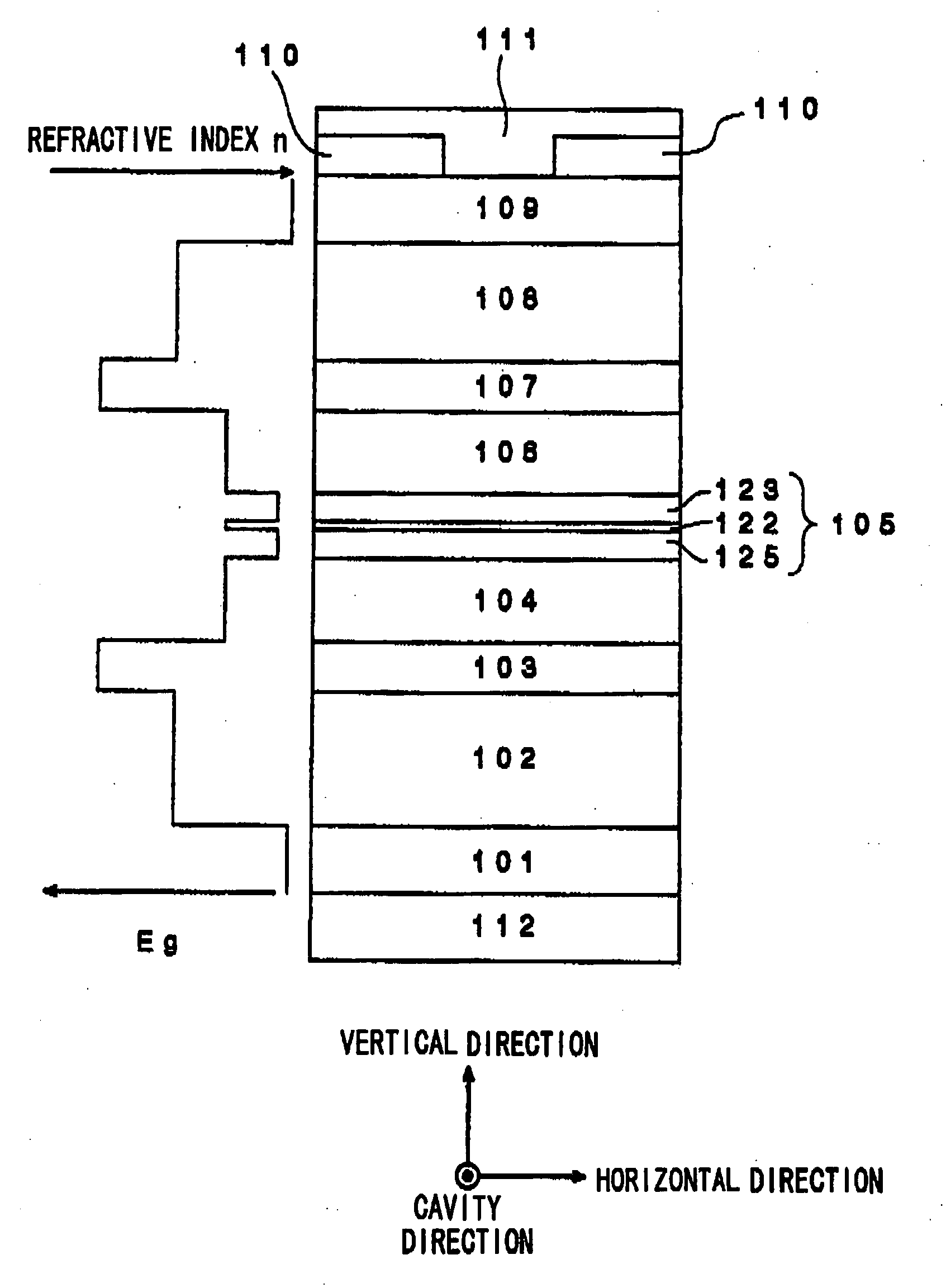
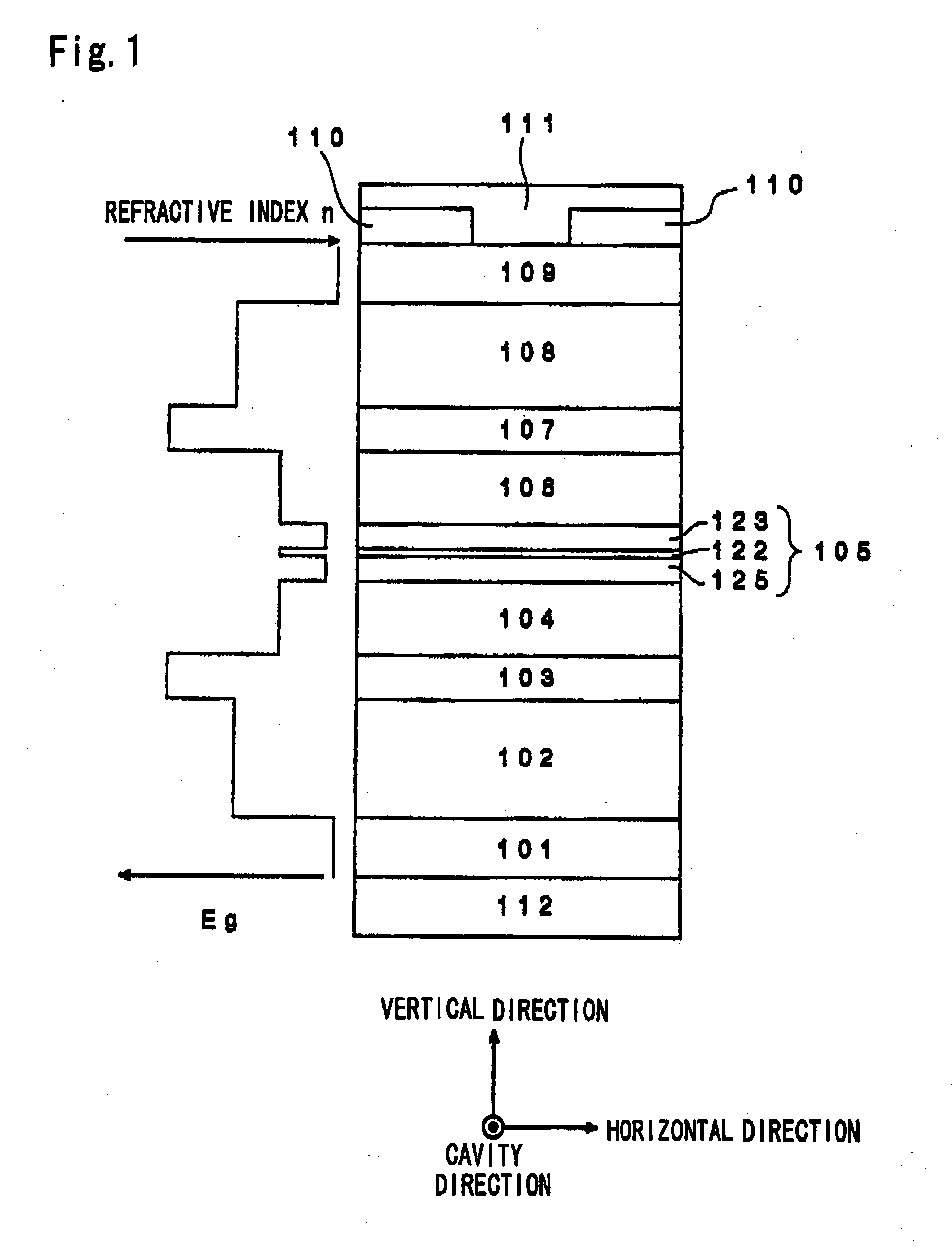
[0266] At first, on the (100) plane of an n-type GaAs substrate (1) at a carrier concentration of 1.0×1018 cm−3, were stacked successively by an MBE method, an Si doped n-type GaAs layer of 0.5 μm thickness at a carrier concentration of 1.0×1018 cm−3 as a buffer layer (2); an Si-doped n-type Al0.19Ga0.92As layer of 2.3 μm thickness at a carrier concentration of 7.5×1017 cm−3 for 1.3 μm from the side of the substrate and 3.0×1017 cm−3 for 1 μm thereover as a first conductive type first clad layer (3); an Si doped n-type Al0.45Ga0.58As layer of 35 nm thickness at a carrier concentration of 8.0×1017 cm−3 as a first-conduction-type second clad layer (4); an GaAs layer of 75 nm thickness at a doping level of Si of 2.0×1017 cm−3 for 35 nm from the side of the substrate and undoped for 40 nm thereover as a first optical guide layer (5) (refracti...
example 2
[0276] Using the device fabricated in Example 1, an optical fiber with a grating, having a fiber lens of a wedged top end, was mounted on the side of the front facet of the device to fabricate a semiconductor laser module having a butterfly type package. The grating fiber has a reflection center of 982 nm and a reflectivity of 3%. At 25° C., the threshold current was 27.6 mA and the slope efficiency was 0.71 mW / mA for the light emitted from the fiber end. The coupling efficiency was good as about 81.6%.
example 3
[0277] A semiconductor laser was fabricated by following procedures.
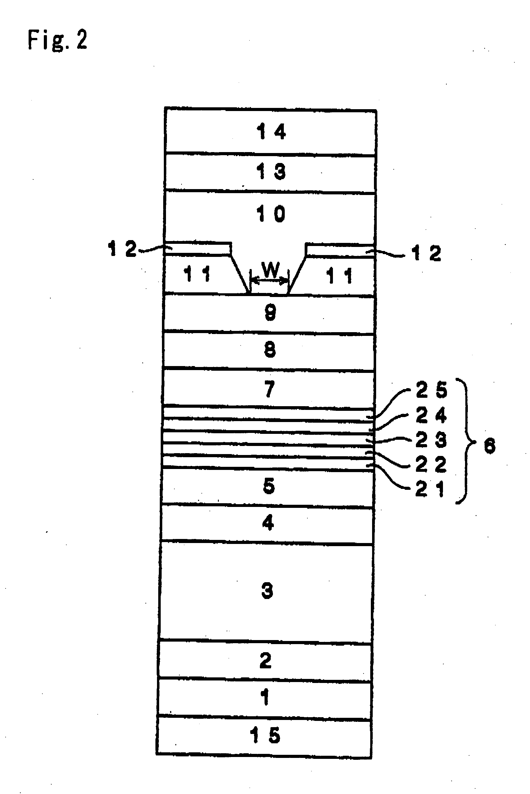
[0278] At first, on the (100) plane of an n-type GaAs substrate at a carrier concentration of 1.0×1018 cm−3, were stacked successively by an MBE method, an Si doped n-type GaAs layer of 1 μm thickness at a carrier concentration of 1.0×1018 cm−3 as a buffer layer; an Si-doped n-type Al0.175Ga0.825As layer of 2.5 μm thickness at a carrier concentration of 6.0×1017 cm−3 for 1.5 μm from the side of the substrate and 4.0×1017 cm−3 for 1 μm thereover as a first conductive type first clad layer; then, an Si-doped n-type AltGa1-tAs layer of 35 nm thickness at a carrier concentration of 5.0×1017 cm−3 in which the Al composition is; t=0.175 on the side of the first-conduction-type first clad layer and the Al composition increases therefrom linearly in the layer up to: t=0.35 on the side of the first-conduction-type second clad layer as the first conduction type transition layer; an Si doped n-type Al0.35Ga0.65As layer of 35 ...
PUM
 Abstract
Description
Claims
Application Information