Hardenable composition, hardening product, process for producing the same and light emitting diode sealed with the hardening product

a technology of hardening product and composition, which is applied in the field of curing product and curing composition, can solve the problems of low toughness of sealant resin, low adhesion properties, and low credibility of final products, and achieve excellent adhesion properties, high transparency, and excellent adhesion properties

Inactive Publication Date: 2005-09-22
KANEKA CORP
View PDF4 Cites 49 Cited by
  • Summary
  • Abstract
  • Description
  • Claims
  • Application Information

AI Technical Summary

Benefits of technology

[0008] Accordingly, the first object of the present invention is to provide a curable composition providing a curing product excellent in adhesive properties and high in transparency, and/or a curable composition providing a curing product excellent in adhesive properties, and high in toughness and transparency; a curing product obtainable by curing said curable composition; a process for producing said curing product; and a light-emitting diode using said curing product. The second and third objects of the present invention are to provide

Problems solved by technology

When the adhesive properties are low, peeling occurs between an LED package and a sealant resin surface.
By the occurrence of peeling, reflectivity may decrease, or in the case where the adhesive properties are significantly low, a sealant resin may possibly become unstuck from the package, thus leading to problems on credibility of final products.
When the toughness of the sealant resin is low, for example, problems such as generation of a crack in reflowing a solder at the time of packaging an LED occur.
Furthermore, problems such as generation of a crack due to irresistible change of using environment e.g. temperature change from high temperatures to low temperatures, etc. may also occur.
From the hardness, tucking ability, and optical characteristics viewpoint, however, the materials obtained by this technology are not suited for use as the transparent optical material, particularly the light-emitting diodes.
However, there is no disclosure therein abo

Method used


Image

  • Hardenable composition, hardening product, process for producing the same and light emitting diode sealed with the hardening product
  • Hardenable composition, hardening product, process for producing the same and light emitting diode sealed with the hardening product
  • Hardenable composition, hardening product, process for producing the same and light emitting diode sealed with the hardening product

Examples


synthesis example 1

(Synthesis Example 1)

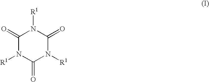
[0422] A 5-L separable flask was charged with 1.8 kg of toluene and 1.44 kg of 1,3,5,7-tetramethylcyclotetrasiloxane, and heated until the inside temperature arrived at 104° C. Thereto was added dropwise a mixture of 200 g of triallyl isocyanurate, 1.44 mL of platinum-vinylsiloxane complex solution in xylene (containing 3% by weight of platinum) and 200 g of toluene. The resulting mixture was heated under reflux in an oil bath at 120° C. for 7 hours. Then, 1.7 g of 1-ethynyl-1-cyclohexanol was added. The unreacted portion of 1,3,5,7-tetramethylcyclotetrasiloxane and the toluene were distilled off under reduced pressure. 1H-NMR revealed that the product was the reaction product resulting from part of the SiH groups of 1,3,5,7-tetramethylcyclotetrasiloxane with triallyl isocyanurate (hereinafter referred to as partial reaction product B1, SiH value: 8.2 mmol / g, allyl value: 0.12 mmol / g) The product is a mixture but contains, as a main component, the compound havin...

example 1

(Measurement Example 1)

[0426] The one-pot mixtures prepared in Example 1, and Comparative Examples 1 and 2 were applied on an aluminum plate (A-1050P) to prepare coating films of approximately 20 μm, and the films were heated at 120° C. for 1 hour. The optical materials were colorless and transparent. After cooling the films to room temperature, adhesion property test was carried out according to JISK 5400 cross-cut taping method (25 grids of 2 mm square) The obtained results are shown in Table 1.

(Measurement Example 2)

[0427] For the curing products obtained in Example 1, and Comparative Examples 1 and 2, a heat and light resistance test was carried out using Suga Test Instruments' M6T-type metering weatherometer (black panel temperature 120° C., irradiation intensity: 50 MJ / m2), and coloration and the light transmittance at 470 nm using a spectrophotometer (U-3300, Hitachi, Ltd.) were determined before and after the test. The obtained results are shown in Table 1.

TABLE 1Example...

example 2

(Example 2)

[0429] The sheet-shaped curing product produced in Example 1 is cut into an appropriate form, and fixed on a light-transmitting window disposed on a metal cap for can type. Meanwhile, a light emitting element having a double-hetero structure in which an Si- and Zn-doped InGaN active layer formed on a sapphire substrate by MOCVD (Metal Organic Chemical Vapor Deposition) method being sandwiched with n- and p-type AlGaN clad layers is prepared. Successively, this light emitting element is mounted on a metal stem for can type, and p- and n-electrodes were wire-bonded with an Au line to the respective leads. This is air-sealed with the above metal cap for can type. In this manner, a can type light-emitting diode can be produced.

(Example 3)

[0430] On a washed sapphire substrate, by MOCVD (Metal Organic Chemical Vapor Deposition) method, the below-mentioned layers are laminated in the following order: n-type GaN layer which is an undoped nitride semiconductor; GaN layer which i...


PUM

PropertyMeasurementUnit
Fractionaaaaaaaaaa
Fractionaaaaaaaaaa
Percent by massaaaaaaaaaa

Abstract

The present invention provides a curable composition providing a curing product having excellent adhesive properties and high transparency, or a curing product having high toughness and transparency. A curable composition which contains (A) an organic compound containing at least two carbon-carbon double bonds reactive with a SiH group in each molecule, (B) a silicon compound having at least two SiH groups in each molecule, (C) a hydrosilylation catalyst, (D) a silane coupling agent and/or an epoxy group-containing compound, and (E) a silanol condensation catalyst. A light-emitting diode sealed with a curing product obtainable by curing said curable composition.

Description

TECHNICAL FIELD [0001] The present invention relates to a curable composition, a curing product thereof, a process for producing the curing product, and a light-emitting diode sealed with the curing product. BACKGROUND ART [0002] As an optical material including a sealing material for light-emitting diodes (LED), with the change of using environment in recent years, those having not only high optical transparency but also high adhesive properties have been demanded. When the adhesive properties are low, peeling occurs between an LED package and a sealant resin surface. By the occurrence of peeling, reflectivity may decrease, or in the case where the adhesive properties are significantly low, a sealant resin may possibly become unstuck from the package, thus leading to problems on credibility of final products. For example, a surface-packaged type LED is desired to have preferable adhesive properties with package constituent materials such as plastic, ceramics and silver. [0003] On t...

Claims


Application Information

Patent Timeline
IPC IPC(8): C08F8/00C08F8/42C08G77/42C08G77/50C08G77/54C08K5/54C08L63/00C08L83/00C08L83/05C08L83/10C08L83/14H01L33/56
CPCC08F8/42C08G77/12H01L2924/0002H01L33/56C08L83/14C08G77/42C08G77/50C08G77/54C08K5/54C08L63/00C08L83/10C08L83/04H01L2924/00Y10T428/31663
Inventor TSUMURA, MANABUIDE, MASAHITOOUCHI, KATSUYAKURAMOTO, MASUFUMIMIKI, TOMOHIDENII, IKUYA
Owner KANEKA CORP
Why Eureka
Try Eureka