Method for manufacturing semiconductor device

a manufacturing method and semiconductor technology, applied in the direction of semiconductor devices, basic electric elements, electrical equipment, etc., can solve the problems of difficult to continue manufacturing semiconductor elements, peeling layers tend to be peeled from the substrate, and flexible substrates such as plastic substrates may not have such high heat resistance, so as to achieve the effect of rapidly peeling semiconductor elements

Inactive Publication Date: 2005-09-29
SEMICON ENERGY LAB CO LTD
View PDF15 Cites 73 Cited by
  • Summary
  • Abstract
  • Description
  • Claims
  • Application Information

AI Technical Summary

Benefits of technology

[0008] It is an object of the present invention to provide a method for manufacturing a semiconductor device, capable of keeping a peeling layer from being peeled from a substrate in the phase before the completion of a semiconductor element and peeling a semiconductor element rapidly.

Problems solved by technology

However, a flexible substrate such as a plastic substrate may often not have such a high heat resistance that it can withstand heat treatment during a step of manufacturing a semiconductor element.
However, in the step of manufacturing a semiconductor element, there is a problem that the peeling layer tends to be peeled from the substrate when heat treatment of the peeling layer is performed in the process of manufacturing the semiconductor element.
After completing the semiconductor element, the peeling layer is peeled from the substrate in the end; however, it is difficult to continue manufacturing the semiconductor element when the peeling layer is peeled from the substrate before the semiconductor element is completed.

Method used


Image

  • Method for manufacturing semiconductor device
  • Method for manufacturing semiconductor device
  • Method for manufacturing semiconductor device

Examples


embodiment 1

[Embodiment 1]

[0057] Next, this embodiment describes a detailed method for manufacturing an ID chip which is one of semiconductor devices employing a manufacturing method of the present invention. Note that this embodiment shows an insulated TFT as an example of semiconductor elements; however, a semiconductor element used for an integrated circuit is not limited thereto and all circuit elements can be used.

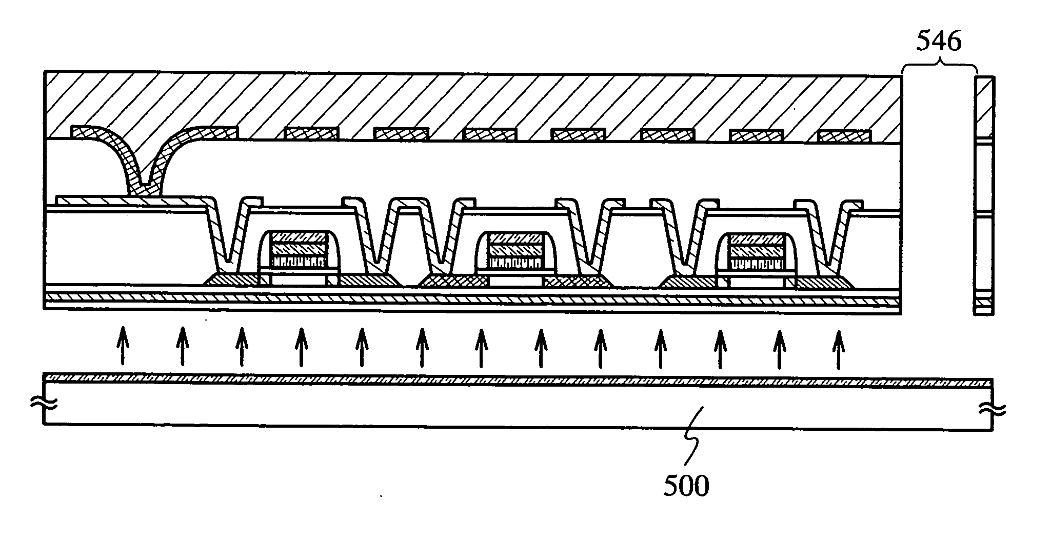
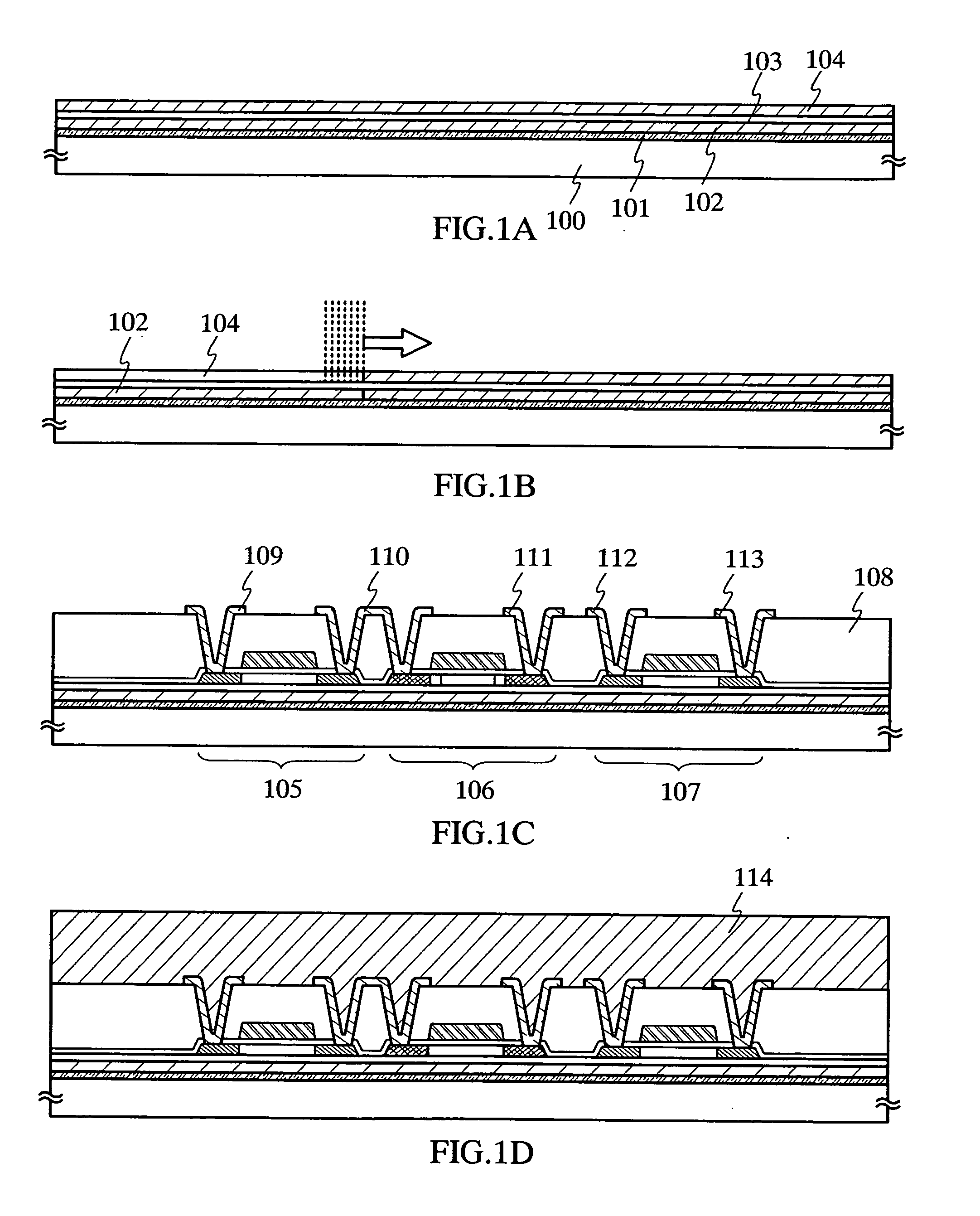
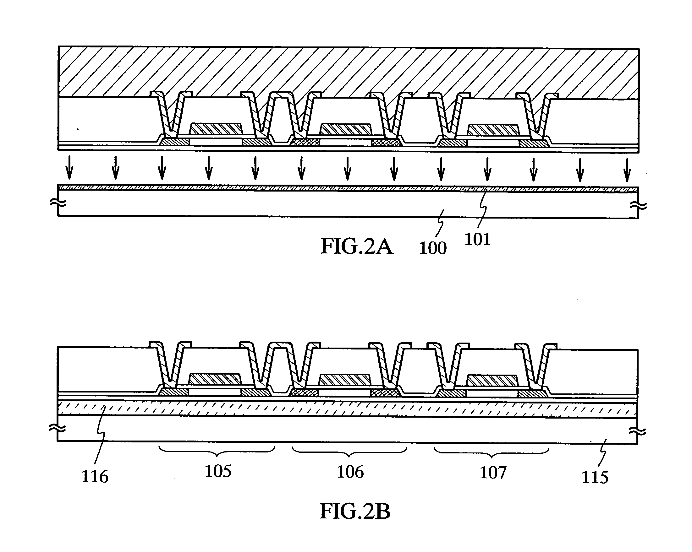
[0058] First, as shown in FIG. 3A, a buffer film 501 is formed on a heat-resistant first substrate 500. For example, a glass substrate such as a barium borosilicate glass or an alumino borosilicate glass, a quartz substrate, a ceramic substrate, or the like can be used for the first substrate 500. Alternatively, a metal substrate including a stainless substrate or a semiconductor substrate may also be used. Although a substrate made of flexible synthetic resin such as plastics generally tends to be inferior in heat-resistant temperature as compared with the above substrates, the...

embodiment 2

[Embodiment 2]

[0134] This embodiment describes an optical micrograph of the sample in which a peeling layer is etched after crystallizing it by performing laser crystallization of a semiconductor film with a continuous-wave laser.

[0135] The sample used in this embodiment is formed by sequentially laminating a buffer film, a peeling layer, a base film, and a semiconductor film over a glass substrate; then crystallizing the semiconductor film by using a catalyst element; further the semiconductor film is partially crystallized with a continuous-wave laser; and then the crystallized semiconductor film is removed by etching. Then, a groove is formed by scribing, and thus, the peeling layer is exposed and etched partially.

[0136] Specifically, the buffer film made of 100 nm thick silicon oxynitride is formed over a glass substrate by using a sputtering method, and the peeling layer made of 50 nm amorphous silicon is formed over the buffer film by using a plasma CVD method to form each s...

embodiment 3

[Embodiment 3]

[0141] A structure of an ID chip in the case of forming a wiring and an antenna connected to a TFT concurrently by patterning a conductive film is described with reference to FIG. 12A. FIG. 12A shows a cross-sectional view of the ID chip in this embodiment.

[0142] In FIG. 12A, a TFT 1401 includes an island-shape semiconductor film 1402, a gate insulating film 1403 being in contact with the island-shape semiconductor film 1402, and a gate electrode 1404 overlapped with the island-shape semiconductor film 1402 by sandwiching the gate insulating film 1403 therebetween. In addition, the TFT 1401 is covered with a first interlayer insulating film 1405 and a second interlayer insulating film 1406. Note that the TFT 1401 is covered with the two interlayer insulating films of the first interlayer insulating film 1405 and the second interlayer insulating film 1406 in this embodiment; however, this embodiment is not limited to this structure. The TFT 1401 may be covered with a s...


PUM


Abstract

It is an object of the present invention to provide a method for manufacturing a semiconductor device, capable of keeping a peeling layer from being peeled from a substrate in the phase before the completion of a semiconductor element and peeling a semiconductor element rapidly. It is considered that a peeling layer tends to be peeled from a substrate because the stress is applied to a peeling layer due to the difference in thermal expansion coefficient between a substrate and a peeling layer, or because the volume of a peeling layer is reduced and thus the stress is applied thereto by crystallization of the peeling layer due to heat treatment. Therefore, according to one feature of the invention, the adhesion of a substrate and a peeling layer is enhanced by forming an insulating film (buffer film) for relieving the stress on the peeling layer between the substrate and the peeling layer before forming the peeling layer over the substrate.

Description

BACKGROUND OF THE INVENTION [0001] 1. Field of the Invention [0002] The present invention relates to a method for manufacturing a semiconductor device in which a semiconductor element formed on an insulating surface is peeled. [0003] 2. Description of the Related Art [0004] A flexible substrate such as a plastic substrate is superior to a glass substrate in terms of mechanical strength against vibration and impact, and the thickness is easily reduced. In addition, the shape of the flexible substrate has higher possibility compared with a glass substrate. Therefore, various applications of a semiconductor device using the flexible substrate are expected. However, a flexible substrate such as a plastic substrate may often not have such a high heat resistance that it can withstand heat treatment during a step of manufacturing a semiconductor element. Accordingly, a manufacturing method in which a semiconductor element formed over a heat-resistant substrate is peeled and attached to a f...

Claims


Application Information

Patent Timeline
Patent Type & Authority Applications(United States)
IPC IPC(8): H01L21/46H01L21/58H01L21/68H01L21/77H01L21/84H01L27/12
CPCH01L21/6835H01L27/1214H01L2221/6835H01L2221/68368H01L2924/19041H01L2224/83H01L24/83H01L2924/3025H01L2924/01029H01L2924/3512H01L2924/00H01L2924/15787H01L2924/12042H01L2924/12044H01L2924/12041H01L2924/14H01L27/1218H01L27/1266
Inventor MARUYAMA, JUNYAISOBE, ATSUOOKAZAKI, SUSUMUTANAKA, KOICHIROYAMAMOTO, YOSHIAKIDAIRIKI, KOJITAMURA, TOMOKO
Owner SEMICON ENERGY LAB CO LTD
Why Eureka
Try Eureka