Organic photoelectric conversion element and method of producing the same, organic photodiode and image sensor using the same, organic diode and method of producing the same

a conversion element and organic technology, applied in the field of methods, can solve the problems of short product life, difficulty in cost reduction, and currently available organic photoelectric conversion elements cannot meet the life requirement of any type of application, and achieve the effects of reducing the dark current of an organic photodiode, high sensitivity, and high performance information read-ou

Inactive Publication Date: 2005-10-06
PANASONIC CORP
View PDF23 Cites 144 Cited by
  • Summary
  • Abstract
  • Description
  • Claims
  • Application Information

AI Technical Summary

Benefits of technology

[0023] An object of the present invention is to provide a long life organic photoelectric conversion element together with the intention of performance stabilization. Another object of the invention is to reduce the dark current of organic photodiodes and to provide an image sensor having a high sensitivity. Moreover, the invention provides an organic diode which reduces the reverse bias current and has a high rectification ratio, and the production method of the same.

Problems solved by technology

However, recently there arises a serious problem with such an inorganic solar cell acting as a clean electric power generator with respect to the environmental load for waste disposal.
However, the above-described organic photoelectric conversion element has had a problem of being liable to undergo performance deterioration, leading to a short product life.
Namely, there has been a problem that, in cases where the organic photoelectric conversion element is used as a product such as a solar cell or photo sensor, the currently available organic photoelectric conversion element cannot sufficiently satisfy life requirement for any type of application, though the life required for each of these products is different.
Such an inorganic material-based photo-receptive part involves the problem of the difficulty in cost reduction because the manufacture of the photo-receptive part requires large-scale semiconductor processes and a large number of steps, and moreover because area expansion is difficult.
But, in the case where carrier leakage between the contiguous photo-receptive parts are negligible due to the low carrier mobility of the organic material, the organic material may be formed in the entire area without any patterning whereby individual photoreceptive parts are not separated from each other.
However, the conventional organic photodiode was not suited for the applications requiring high-speed, high-sensitivity image sensors since the organic photodiode had a very large dark current.
In some cases, detection of the charge amount reduced by light irradiation becomes quite difficult.
Since the conventional organic photodiode suffered from a large dark current, there were problems that the resulting S / N ratio is small and that only low-sensitivity image sensor can be produced.
In particular, in the BH-type element, the influence of the dark current discussed above is serious, and the solution of the problem has been a pressing need.
Now, various electronic parts required for electric circuits such as a diode, condenser, resistor and transistor can be constituted with organic semiconductor materials, but their characteristics are not at the level of full satisfaction as yet.
Therefore, if there exists a thin part or defect in the layer, the leak current becomes large under reverse bias application, resulting in a small rectification ratio.
This problem particularly seriously influences the performance of the BH-type organic diode, and the solution thereof is urgently demanded.

Method used


Image

  • Organic photoelectric conversion element and method of producing the same, organic photodiode and image sensor using the same, organic diode and method of producing the same
  • Organic photoelectric conversion element and method of producing the same, organic photodiode and image sensor using the same, organic diode and method of producing the same
  • Organic photoelectric conversion element and method of producing the same, organic photodiode and image sensor using the same, organic diode and method of producing the same

Examples


embodiment 1

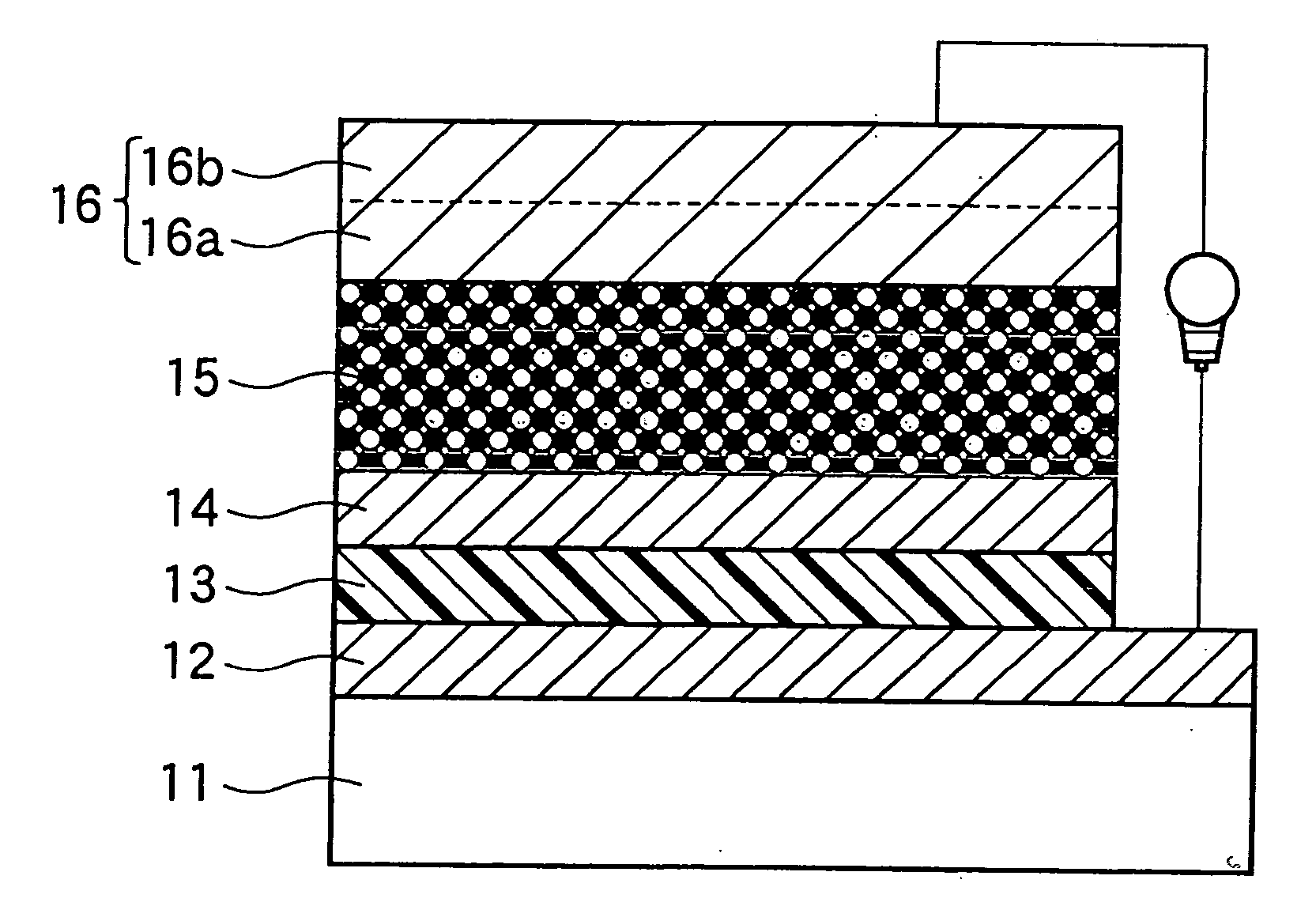
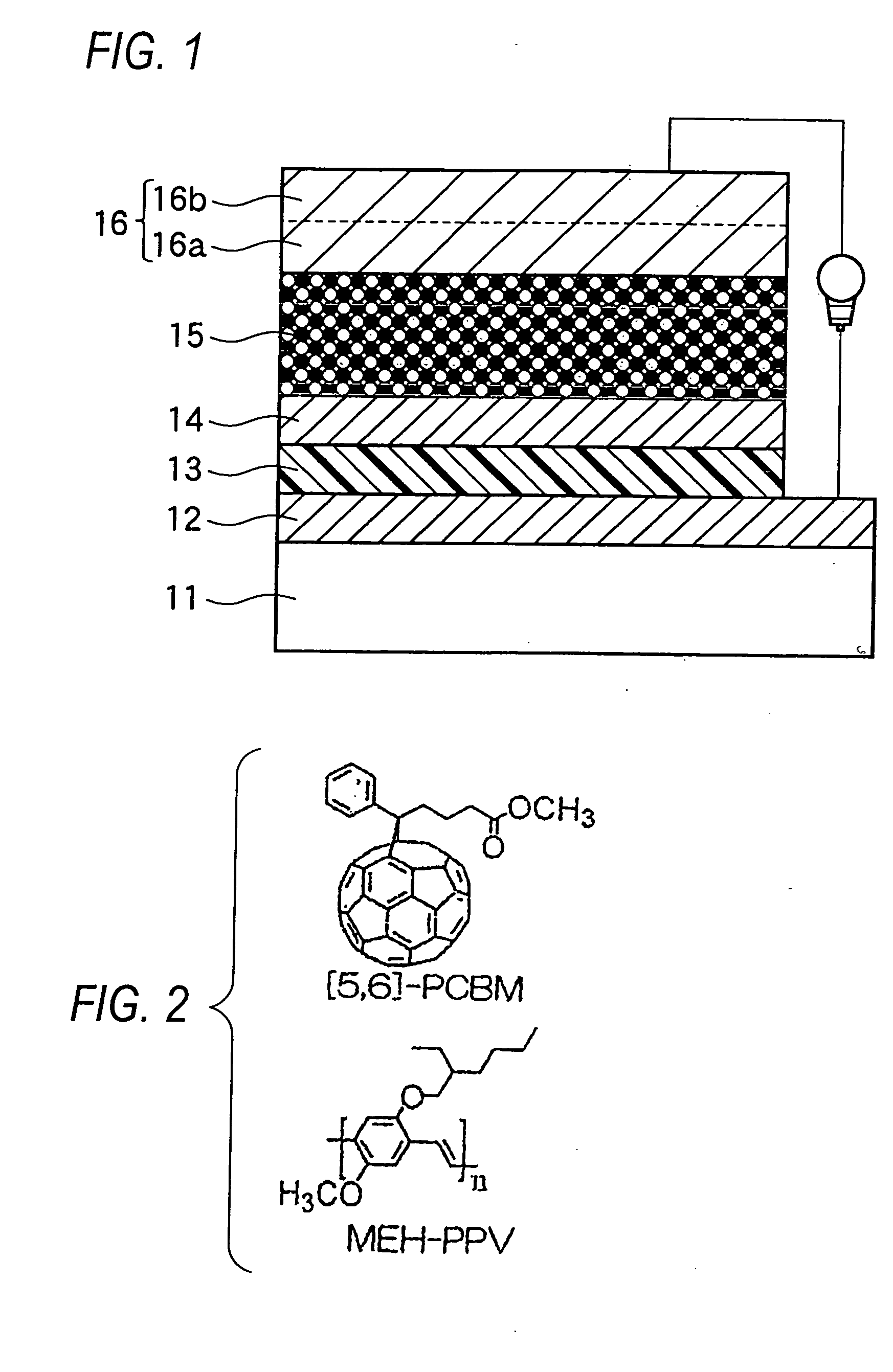
[0098] One embodiment of the invention is described in detail with reference to the drawings. The present embodiment is characterized by that a buffer layer 14 comprising an inorganic film made of molybdenum oxide (MoO3) is arranged between an organic photoelectric conversion layer 15 and a positive electrode 12, as shown in FIG. 1.

[0099] Namely, as shown in FIG. 1, the buffer layer 14 comprising an inorganic matter is inserted between the charge transport layer 13 and the organic photoelectric conversion layer 15 for the purpose of preventing the diffusion of the materials constituting the charge transport layer 13, particularly ionic materials into the organic photoelectric conversion layer 15. Thus, on a substrate 11, a positive electrode 12, a charge transport layer 13, a buffer layer 14, an organic photoelectric conversion layer 15 and a negative electrode 16 are stacked in this order.

[0100] With this configuration, an organic photoelectric conversion element showing high eff...

example 1

[0125] Next, an example is described. First of all, on a glass substrate 11, an ITO film 12 with 150 nm thickness was formed by means of sputtering. Thereafter, on this ITO film a resist film with 5 μm thickness was provided by spin-coating a resist material (OFPR-800 of Tokyo Ohka Kogyo Co., Ltd.). Then, via masking, exposure and development, the resist film was patterned into the shape of a positive electrode 12.

[0126] Then, after immersed in an 18 N aqueous hydrochloric acid kept at 60° C. to etch the ITO film 12 at the portion where no resist film is present, this glass substrate was washed with water. Finally, by removing the resist film, a positive electrode 12 consisting of the ITO film in the pre-determined pattern was obtained.

[0127] Then, the glass substrate 11 was subjected to ultrasonic rinsing with a detergent (Semico-clean, a product of Furuuchi Chemical Corp.) for 5 min, ultrasonic rinsing with pure water for 10 min, ultrasonic rinsing for 5 min with a solution obta...

embodiment 2

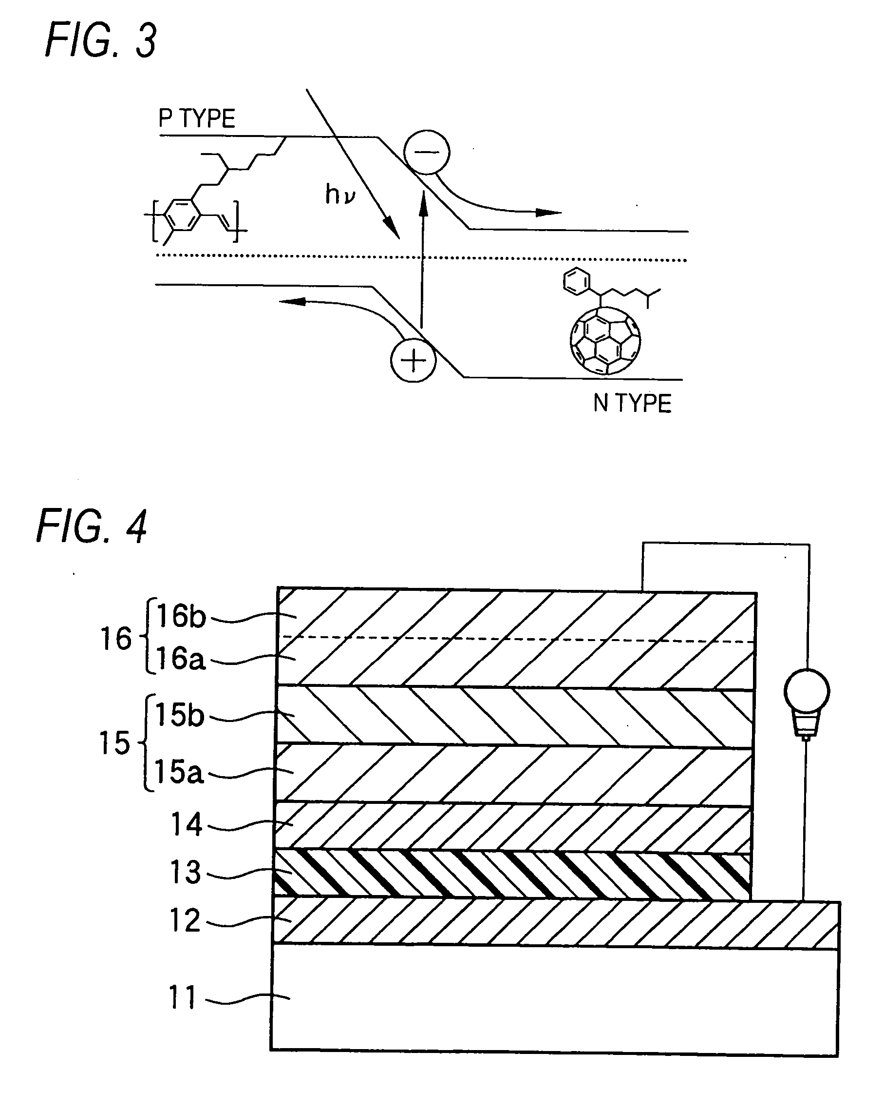
[0136] Next, Embodiment 2 for practicing the invention is described. While, in the foregoing Embodiment 1, the organic photoelectric conversion layer consisted of a mono-layer containing an electron donating material and an electron accepting material, the present embodiment adopts a dual-layer structure comprising an electron accepting layer 15 a and an electron donating layer 15b as shown in FIG. 4 wherein a pn junction is formed at the interface of the two layers. The other portions are structurally the same as those of the organic photoelectric conversion element set forth in the aforementioned Embodiment 1.

[0137] In the organic photoelectric conversion element of such a structure, the transfer of carriers is limited to occur only at the pn junction. Therefore, the excitons generated in the inside of the electron donating layer far from the junction cannot deliver electrons to the electron accepting material. Hence, such a phenomenon may exert an adverse effect on the PEDOT:PSS...


PUM

PropertyMeasurementUnit
thicknessaaaaaaaaaa
thicknessaaaaaaaaaa
thicknessaaaaaaaaaa

Abstract

The organic photoelectric conversion element in accordance with the invention comprises at least one pair of electrodes 12 and 16, a photoelectric conversion region (layer) 15 arranged between the electrodes and containing at least an electron donating organic material and an electron accepting organic material, and a buffer layer 14 containing at least one inorganic matter and inserted between the photoelectric conversion region and at least one electrode of the above-cited pair of electrodes.

Description

BACKGROUND OF THE INVENTION [0001] 1. Field of the Invention [0002] The present invention relates to an organic photoelectric conversion element, a method of producing the same, and, in particular, an organic photoelectric conversion element having stable characteristics in expectation of the application to solar cells and photo-sensors. Further, the present invention relates to an organic photodiode capable of converting light to electricity by making use of the pn junction of organic semiconductor materials, and an image sensor using the same and capable of reading the information of documents as well as substances. Furthermore, the present invention relates to an organic diode and a method of producing the same, and in particular such an organic diode that has high rectification property in expectation of the application to electronic parts. [0003] 2. Related Art [0004] An inorganic solar cell using silicon such as amorphous silicon is a clean device which is under study for prac...

Claims


Application Information

Patent Timeline
Patent Type & Authority Applications(United States)
IPC IPC(8): H01L21/314H01L27/30H01L51/00H01L51/30H01L51/42H01L51/44
CPCB82Y10/00H01L21/3146H01L27/305H01L27/307H01L51/0038Y02E10/549H01L51/0048H01L51/0052H01L51/424H01L51/4253H01L51/442H01L51/0046H10K39/30H10K39/32H10K85/114H10K85/211H10K85/221H10K85/615H10K30/20H10K30/30H10K30/82H01L21/02115
Inventor KOMATSU, TAKAHIROSAKANOUE, KEIYATSUNAMI, RYUICHIMIZUSAKI, MASAKAZUKITADA, TAKASHIINOUE, MASAHIRO
Owner PANASONIC CORP
Why Eureka
Try Eureka