Method of producing optical disk-use original and method of producing optical disk
a technology of optical discs and originals, applied in the direction of optical recording/reproducing/erasing methods, instruments, photosensitive materials, etc., can solve the problem of long development steps and achieve the effect of high-precision resist patterns
- Summary
- Abstract
- Description
- Claims
- Application Information
AI Technical Summary
Benefits of technology
Problems solved by technology
Method used
Image
Examples
example 1
[0106] In Example 1, a master having a resist thereon (i.e., resist master) used for producing an optical disc was actually produced using a resist material composed of an incomplete oxide of trivalent tungsten (W).
[0107] A resist layer composed of an incomplete oxide of tungsten was uniformly deposited by sputtering on a glass substrate having a sufficiently smooth surface. The sputtering was performed with a sputtering target composed of tungsten element in an atmosphere containing argon and oxygen. The content of oxygen gas was changed in order to control the degree of oxidation of the incomplete oxide of tungsten.
[0108] The composition of the deposited resist layer was analyzed with an energy dispersive X-ray spectrometer (EDX). When the composition ratio was represented by W1-xOx, the value x was 0.63. The thickness of the resist layer was controlled to be 40 nm. The wavelength dependence of the refractive index was measured by spectroscopic ellipsometry.
[0109] The substrate...
example 2
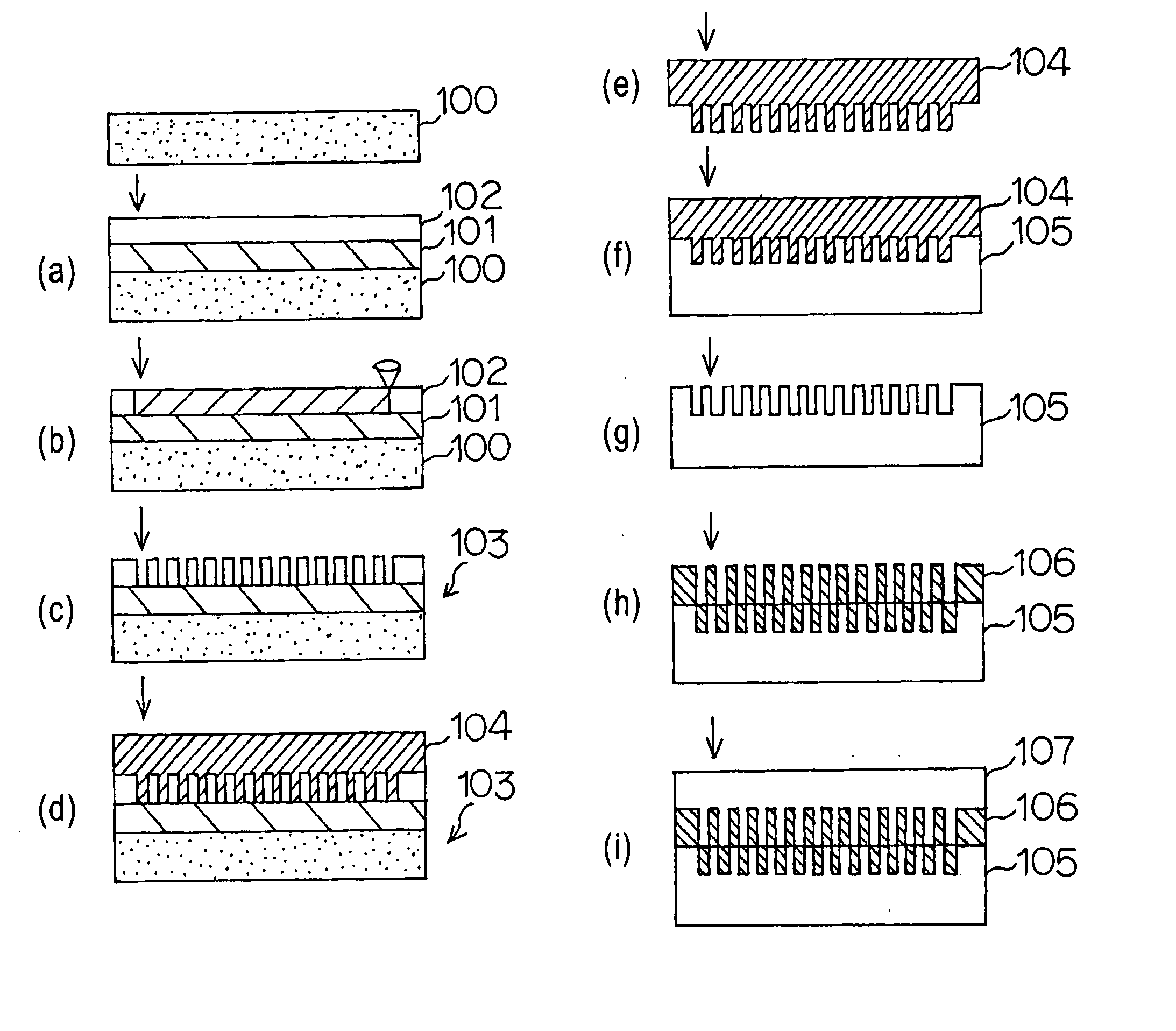
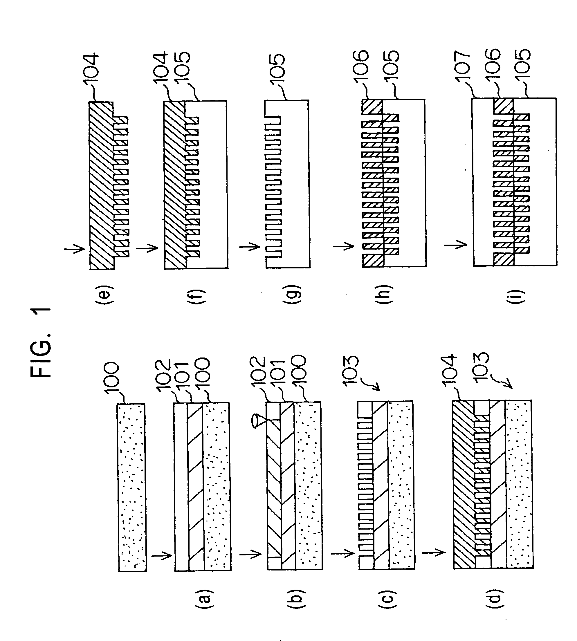
[0118] In Example 2, a resist master used for producing an optical disc was actually produced using a resist material composed of an incomplete oxide of trivalent tungsten and trivalent molybdenum according to the manufacturing process shown in FIG. 1. Then, the optical disc was finally manufactured. The operating process will now be described with reference to FIG. 1.
[0119] Firstly, an interlayer 101 composed of amorphous silicon and having a thickness of 80 nm was uniformly deposited on a substrate 100 that is a silicon wafer by sputtering. Subsequently, a resist layer 102 composed of an incomplete oxide of tungsten (W) and molybdenum (Mo) was uniformly deposited on the substrate by sputtering (FIG. 1(a)). The sputtering was performed in argon atmosphere with a sputtering target composed of the incomplete oxide of tungsten and molybdenum. According to the analytical result of the deposited resist by the EDX, the ratio of the tungsten and molybdenum in the deposited incomplete oxi...
PUM
 Abstract
Description
Claims
Application Information


