Multilayer printed wiring board

a printed wiring and multi-layer technology, applied in the direction of printed element electric connection formation, high-frequency circuit adaptation, printed circuit non-printed electric components association, etc., can solve the problems of high frequency of occurrence of malfunction or error, and ic chip often turning inoperable, etc., to increase the volume of the conductors, increase the strength of the core substrate, and increase the volume

Active Publication Date: 2005-10-27
IBIDEN CO LTD
View PDF4 Cites 60 Cited by
  • Summary
  • Abstract
  • Description
  • Claims
  • Application Information

AI Technical Summary

Benefits of technology

[0010] The first advantage of the invention is that by making the conductor layer as the power supply layer of the core substrate thick, it is possible to intensify the strength of the core substrate and that even if the core substrate itself is made thin, it is possible for the substrate itself to relax warps and generated stresses.
[0011] The second advantage of the invention is that by making the conductor layers thick, it is possible to increase the volumes of the conductors themselves. By increasing the volumes, it is possible to decrease the resistances of the conductors. Due to this, the electrical transmission of the signal line or the like is not hampered. Accordingly, the loss of the signal transmitted or the like does not occur. This advantage is exhibited by making only the substrate which becomes the core thick.
[0012] The third advantage of the invention is that by employing the conductor layer as the power supply layer, it is possible to improve the capability of supplying power to the IC chip. In addition, by employing the conductor layer as the earth layer, it is possible to decrease the noise superposed on the signal and power to the IC chip. This is because the decreased resistances of the conductors as described as the second advantage can prevent the supply of power from being hampered. Due to this, if the IC chip is mounted on the multilayer printed wiring board, it is possible to decrease a loop inductance from the IC chip—the substrate—the power supply. Accordingly, power shortage in an initial operation is decreased to make it difficult to cause power shortage. Even if the IC chip in a higher frequency range is mounted on the multilayer printed wiring board, malfunction, error or the like does not occur in the initial operation.
[0013] Further, even if the power is supplied to the IC chip via the IC chip—the substrate—capacitors or the power supply layer—power, the same advantage can be exhibited. The loop inductance can be decreased. For this reason, no loss occur

Problems solved by technology

However, as the frequency of an IC chip is higher, the frequency of occurrence of malfunction or error becomes higher.
Particularly if the frequency of the IC chip exceeds 3 GHz, the frequency of occurrence of malfunction or error considerably increases.
If the frequency exceeds 5 GHz, the IC chip often t

Method used


Image

  • Multilayer printed wiring board
  • Multilayer printed wiring board
  • Multilayer printed wiring board

Examples


embodiment 1

Glass Epoxy Resin Substrate

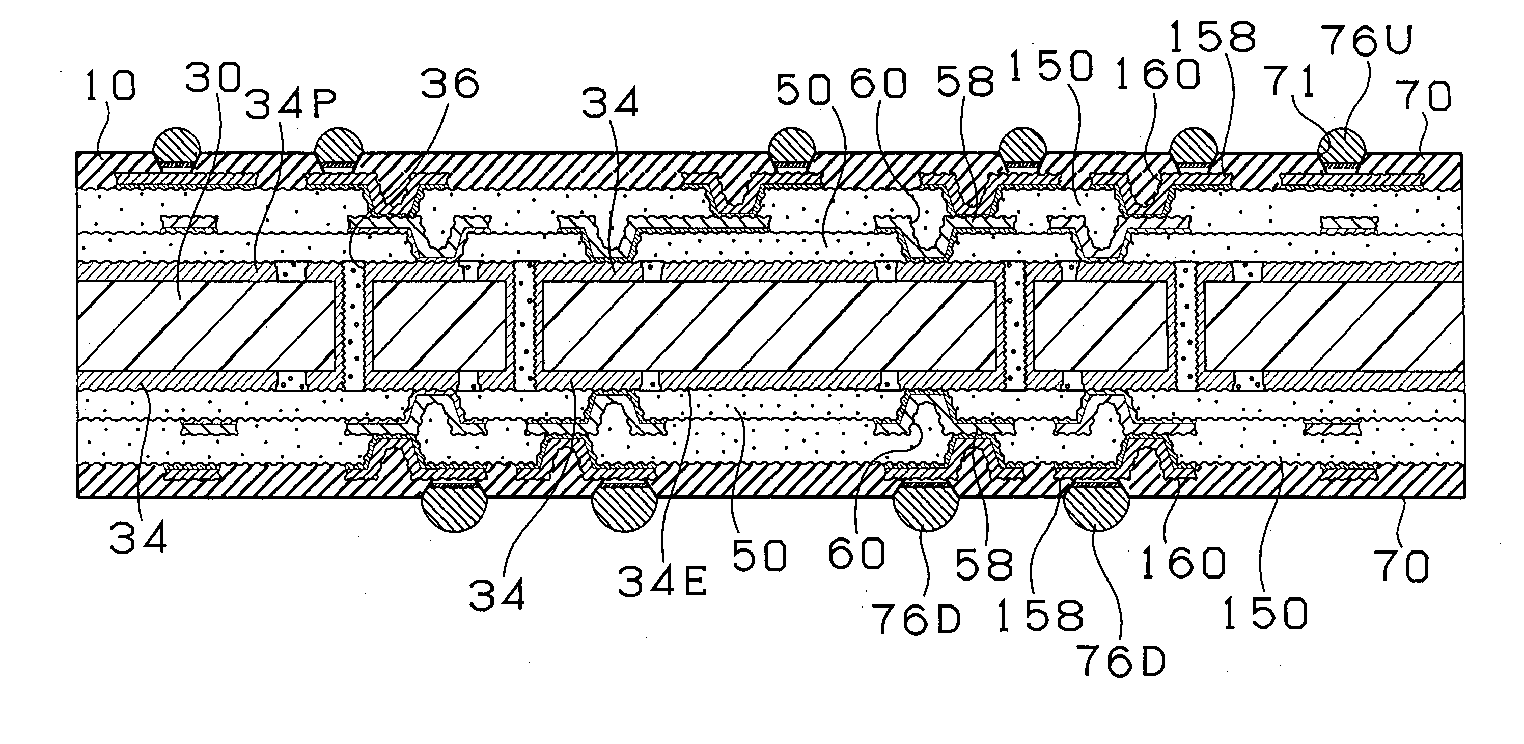
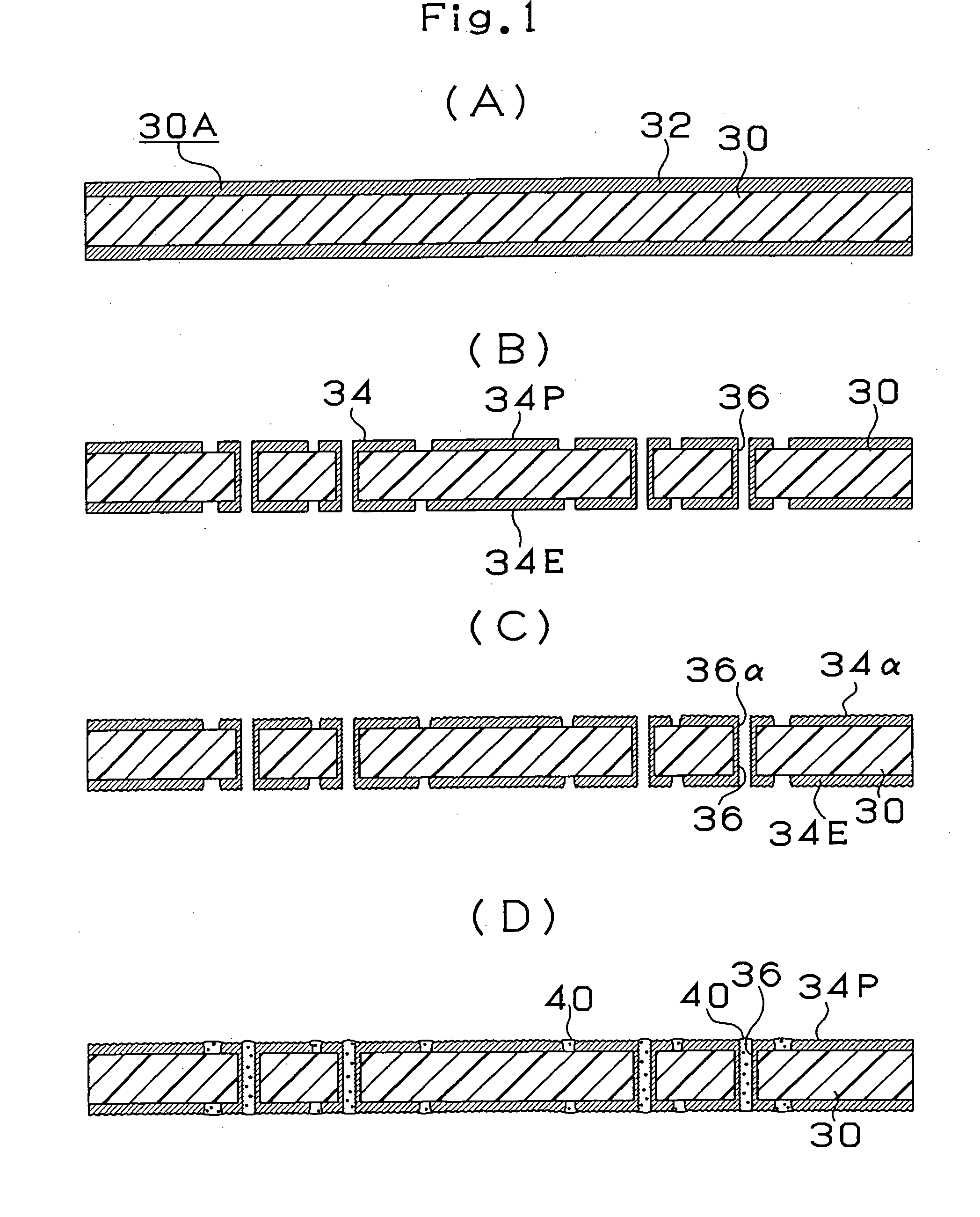
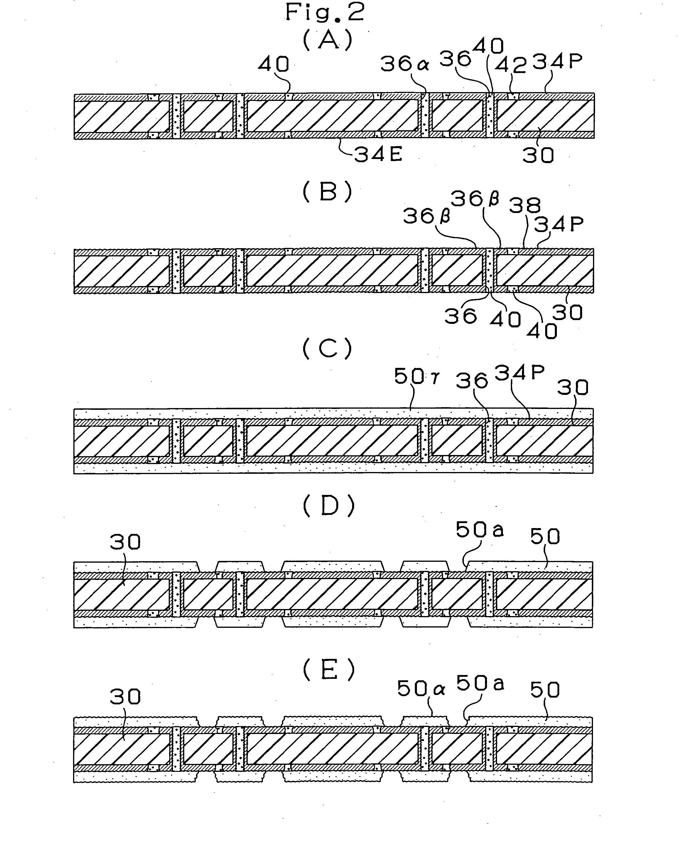
[0072] The configuration of a multilayer printed wiring board 10 according to Embodiment 1 of the present invention will first be described with reference to FIGS. 1 to 7. FIG. 6 shows the cross section of the multilayer printed wiring board 10 and FIG. 7 shows a state in which an IC chip 90 is attached to the multilayer printed wiring board 10 shown in FIG. 6 and in which the board 10 is mounted on a daughter board 94. As shown in FIG. 6, the multilayer printed wiring board 10 has a conductor circuit 34 and a conductor layer 34P formed on the front surface of a core substrate 30, and a conductor circuit 34 and a conductor layer 34E formed on the rear surface of the core substrate 30. The upper conductor layer 34P is formed as a power supply plane layer while the lower conductor layer 34E is formed as an earth plane layer. The front and rear surfaces of the core substrate 30 are connected to each other via through holes 36. In addition, an interlayer resin...

embodiment 1-1

A. Manufacturing of Resin Film of Interlayer Resin Insulating Layer

[0079] 29 parts by weight of bisphenol A type epoxy resin (epoxy equivalent weight of 455, Epicoat 1001 manufactured by Yuka Shell Epoxy), 39 parts by weight of cresol novolac type epoxy resin (epoxy equivalent weight of 215, EpiclonN-673 manufactured by Dainippon Ink and Chemicals) and 30 parts by weight of phenol novolac resin including a triazine structure (phenol hydroxyl group equivalent weight of 120, PhenoliteKA-7052 manufactured by Dainippon Ink and Chemicals) are heated and molten while being agitated with 20 parts by weight of ethyl diglycol acetate and 20 parts by weight of solvent naphtha, and 15 parts by weight of terminally epoxidized polybutadiene rubber (DenalexR-45EPT manufactured by Nagase Chemicals Ltd.) and 1.5 parts by weight of crushed product of 2-phenyl-4,5-bis(hydroxymethyl)imidazole, 2.5 parts by weight of pulverized silica and 0.5 parts by weight of silicon-based defoaming agent are added...

embodiment 1-2

[0110] A multilayer printed wiring board is manufactured in the same manner as that of Embodiment 1-1 described above with reference to FIG. 6 except for the following respects:

[0111] Thickness of conductor layers of a core substrate: 55 μm; thickness of a power supply layer of the core substrate: 55 μm; and thickness of conductor layers of interlayer insulating layers: 15 μm.


PUM


Abstract

A package substrate free of malfunction or error even with an IC chip in a high frequency range, particularly an IC chip with a frequency exceeding 3 GHz, is provided. A conductor layer 34P on a core substrate 30 is formed to have a thickness of 30 μm and a conductor circuit 58 on an interlayer resin insulating layer 50 is formed to have a thickness of 15 μm. By making the conductor layer 34P thick, it is possible to increase a volume of the conductor itself and decrease resistance. Further, by employing the conductor layer 34 as a power supply layer, it is possible to improve a capability of supplying power to the IC chip.

Description

TECHNICAL FIELD [0001] This invention relates to a multilayer printed wiring board and provides a technique related to a multilayer printed wiring board capable of having improved electric characteristics and reliability without causing malfunction, error or the like even if a high frequency IC chip, particularly an IC chip in a high frequency range of 3 GHz or higher is mounted thereon. BACKGROUND ART [0002] In forming a buildup type multilayer printed wiring board constituting an IC chip package, interlayer insulating resin is formed on one of or each of the surfaces of a core substrate having through holes formed therein and via holes for interlayer conduction are opened by a laser or photo etching, whereby an interlayer resin insulating layer is thereby formed. A conductor layer is formed on the via holes by plating or the like and etching and the like are performed to form a pattern, thus creating a conductor circuit. Further, by repeatedly forming the interlayer insulating lay...

Claims


Application Information

Patent Timeline
IPC IPC(8): H01L23/12H01L23/498H05K1/02H05K1/05H05K1/18H05K3/42H05K3/46
CPCH01L23/49816H05K1/09H01L2224/16225H01L2924/01025H01L2924/01046H01L2924/01078H01L2924/01079H01L2924/09701H01L2924/15312H01L2924/19106H01L2924/3011H05K1/0237H05K1/056H05K1/185H05K3/429H05K3/4602H05K3/4608H05K3/4641H05K2201/0347H05K2201/0352H05K2201/09309H05K2201/09536H05K2201/0959H05K2201/096H05K2201/09809H01L2924/01019H05K1/183H01L23/49822H01L2224/05573H01L2224/05568H01L2924/00014H01L2924/15311H01L2924/3511H01L2224/05599H05K3/46H05K1/02
Inventor INAGAKI, YASUSHISANO, KATSUYUKI
Owner IBIDEN CO LTD
Why Eureka
Try Eureka