Inspection method and inspection system using charged particle beam

a technology of inspection system and charged particle, which is applied in the direction of semiconductor/solid-state device testing/measurement, image enhancement, instruments, etc., can solve the problems of unrealistic method, difficult measurement, and soft tip, and achieve the effect of short time only

Inactive Publication Date: 2005-10-27
HITACHI LTD
View PDF9 Cites 1 Cited by
  • Summary
  • Abstract
  • Description
  • Claims
  • Application Information

AI Technical Summary

Benefits of technology

[0011] An object of the invention is to provide an inspection method and system for automatically calculating values of electric resistance and electric capacity and obtaining distributions and tendencies of electric resistance and electric capacity of the surface of a substrate such as a wafer in short time only by acquiring a voltage contrast image. Another object is to provide appropriate inspection parameters corresponding to the structure of a wafer.
[0022] Further, a method of providing appropriate inspection parameters adapted to the structure of a wafer will now be described. FIG. 8 shows that the NSE changes by changing the retarding voltage VR. In this case, the charging voltage US (V) in an electron beam irradiation region also varies as shown in FIG. 24. The phenomenon is used for the inspection. For example, when a circuit pattern having a pn junction is irradiated with an electron beam and the pn junction is charged so as to be reverse-biased, the junction has high resistance, and it is consequently difficult to discriminate the junction from a defect of faulty electrical continuity. However, by changing the retarding voltage to increase the charging voltage and to cause a breakdown in the pn junction, the resistance value can be reduced. Since the difference between the resistance value in the normal portion and the resistance value in the defective portion becomes large and the normal portion and the defective portion become different from each other in a voltage contrast image, the inspection can be conducted in such a state.
[0023] In the case where the pn junction itself has a defect and the resistance value in the reverse bias direction is small, the retarding voltage is adjusted to a charging state where a breakdown is caused only in the defective pn junction. The difference between the resistance value in the normal portion and the resistance value in the defective portion is increased, and a difference occurs between the normal and defective portions, so that the inspection can be conducted. Although the retarding voltage is used here, also by changing other electron irradiation parameters such as electron beam current, incident energy of the electron beam to a sample, irradiation time, and the number of irradiation times, similar effects can be produced.
[0028] In the inspection, by changing the current value of the charged particle beam, the measurement range of the electric resistance can be changed. As a process before acquiring an image, the charged particle beam of a predetermined quantity is preliminarily applied or the retarding voltage is applied to the semiconductor wafer, thereby enabling measurement sensitivity to be changed.

Problems solved by technology

As patterns become finer in recent years, however, the size of a portion to be measured becomes about the same or smaller than that of the W needle, so that the measurement is becoming very difficult.
In this case, however, the tip becomes very soft and is consequently deformed when it comes into contact with the portion to be measured.
The method is not a realistic one.
Another problem is contact resistance.
Consequently, accurate measurement cannot be performed.
The technique, however, does not have means for obtaining and displaying electric characteristics (electric resistance and electric capacity) and, therefore, cannot determine whether the portion is critical or not.
However, it takes time for the inspection and the electric resistance cannot be measured at high speed.
In an inspection using such a voltage contrast image of the SEM, in some cases, a difference in potential contrast between the normal portion and the defective portion is small depending on the structure of a wafer, and it is difficult to detect a defect.
Due to this, it is difficult to discriminate the portion from a high-resistant portion with faulty electrical continuity.
As described above, since the nano-probe device has a problem such that a portion to be measured is smaller than the tip of the needle and a problem of the contact resistance between the needle and a sample, accurate electric resistance cannot be measured depending on a sample.
It takes very long time to inspect the whole face of a wafer and is substantially impossible to conduct the inspection.
Although an apparatus using the SEM can determine whether the electric resistance is high or low and whether the electric capacity is large or small from a voltage contrast image but cannot estimate an absolute value.
Although a resistance value can be calculated by measuring a leak current, it takes time for an inspection, the inspection cannot be conducted at high speed, and it takes very long time to inspect the whole face of a wafer.
Further, depending on the structure of a wafer (for example, when a pn junction is formed), it is difficult to discriminate a normal portion from a defective portion in a voltage contrast image.

Method used


Image

  • Inspection method and inspection system using charged particle beam
  • Inspection method and inspection system using charged particle beam
  • Inspection method and inspection system using charged particle beam

Examples


first embodiment

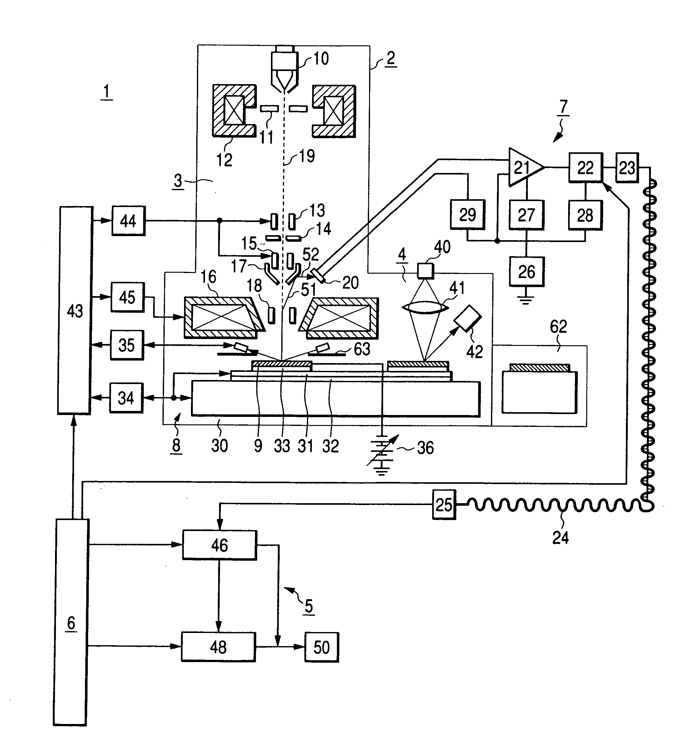
[0059]FIG. 1 shows the configuration of an inspection system as a first embodiment of the invention. The inspection system 1 has an inspection chamber 2 evacuated to be in a vacuum, and a spare chamber (not shown in this embodiment) for carrying a wafer 9 to be inspected into the inspection chamber 2. The spare chamber can be evacuated independent of the inspection chamber 2. The inspection system 1 has, other than the inspection chamber 2 and the spare chamber, a control unit 6 and an image processing unit 5. The inspection chamber 2 has therein, broadly, electron optics 3, a detector 7, a sample chamber 8, and an optical microscope unit 4.

[0060] The electron optics 3 include an electron gun 10, an electron beam extraction electrode 11, a condenser lens 12, a blanking deflector 13, a scanning deflector 15, an aperture 14, an objective lens 16, a converter electrode 17, and an EXB deflector 18. In the detector 7, a detector 20 is disposed above the objective lens 16 in the inspecti...

second embodiment

[0085] In a second embodiment, the electron beam image is acquired by using the inspection system described in the first embodiment and stored in the image memory unit 46. Images of neighboring equivalent circuit patterns are compared with each other by the calculator 48. When a differential signal level is higher than a predetermined value, the portion in the electron beam image is recognized as a defective portion and is displayed. Since the system has been described in detail in the first embodiment, the description will not be repeated. From the image signal level in the defective position, the electric resistance and capacity are calculated by the calculator 48. The degree of difference in resistance or capacity of the defective portion from the normal portion is obtained. There are the following three methods of obtaining an image of the defective portion.

[0086] In a first method, an inspection of comparing the images with each other is conducted. After completion of the insp...

third embodiment

[0091] A third embodiment relates to an inspection method and inspection system for detecting, as a defect, a circuit pattern having resistance different from a predetermined resistance, which is derived from the brightness of an image by obtaining an electron beam image, and simultaneously comparing the brightness of the image in the circuit pattern position with predetermined brightness by using the inspection system described in the first embodiment.

[0092] First, in FIG. 18, a wafer 181 to be inspected is loaded into the inspection system, and pre-registered electron beam irradiation parameters and signal detection parameters are set. On a sample holder 180, a standard sample 182 of which resistance under predetermined electron beam parameters is preliminarily calculated is attached. Before starting the inspection, an image of the standard sample 182 is acquired, and the correspondence between the resistance and capacity and the electron beam image signal level is calibrated.

[0...


PUM

PropertyMeasurementUnit
incident energy EPEaaaaaaaaaa
energyaaaaaaaaaa
potential barrieraaaaaaaaaa

Abstract

Secondary electrons and back scattered electrons generated by irradiating a wafer to be inspected such as a semiconductor wafer with a charged particle beam are detected by a detector. A signal proportional to the number of detected electrons is generated, and an inspection image is formed on the basis of the signal. On the other hand, in consideration of a current value and irradiation energy of a charged particle beam, an electric field on the surface of the inspection wafer, emission efficiency of the secondary electrons and back scattered electrons, and the like, an electric resistance and an electric capacity are determined so as to coincide with those in the inspection image. In a state where a difference between a resistance value in a normal portion and a resistance value in a defective portion is sufficiently increased by using the charging generated by the irradiation of electron beams, an inspection is conducted to thereby detect a defect.

Description

BACKGROUND OF THE INVENTION [0001] The present invention relates to a method and system for manufacturing a wafer having a fine circuit pattern such as a semiconductor device, or liquid crystal. More particularly, the invention relates to a technique of inspecting a pattern of a semiconductor device or a photomask, and to inspecting method and system using a charged particle beam, for inspecting a defect in an arbitrary part on an unfinished semiconductor wafer in a semiconductor device fabricating process. [0002] A semiconductor device is manufactured by, for example, repeating a step of transferring a pattern formed with a photomask on a semiconductor wafer by a lithography process and an etching process. In a manufacturing step of a semiconductor device, whether the lithography process, etching process, and the like are successfully performed or not exerts a large influence on the yield of the semiconductor device. It is consequently important to detect occurrence of an abnormal ...

Claims


Application Information

Patent Timeline
Patent Type & Authority Applications(United States)
IPC IPC(8): G01N21/95G01N23/20G01N21/956G01N23/203G01N23/225G01N27/04G01N27/22G01R1/06G01R31/302G01R31/307G01R31/311G06T7/00H01J37/22H01J37/26H01J37/28H01L21/66H01L31/0336
CPCG01N21/9501G01N23/203G01N23/225G01N2021/95615G01R31/307H01J2237/2817G06T7/001G06T2207/30148H01J37/268H01J37/28G01R31/311
Inventor NISHIYAMA, HIDETOSHINOZOE, MARISHINADA, HIROYUKI
Owner HITACHI LTD
Why Eureka
Try Eureka