

Semiconductor memories
a technology of memory and semiconductors, applied in semiconductor devices, digital storage, instruments, etc., can solve the problems of reducing the area required by the peripheral circuit of memory arrays, and achieve the effects of reducing the size of memory cells, and increasing the retention tim
- Summary
- Abstract
- Description
- Claims
- Application Information
AI Technical Summary
Benefits of technology
Problems solved by technology
Method used
Image

Examples
second embodiment
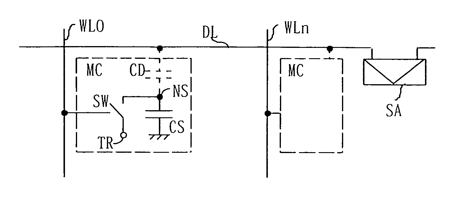
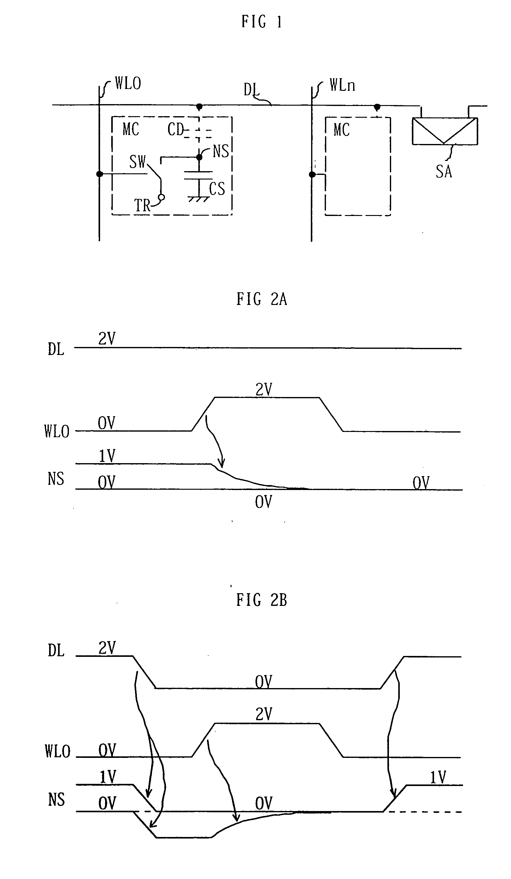
[0095] In this embodiment, two dummy cells DC are preferably included in each column with the output of one dummy cell connected to one of a pair of data lines D0, D1, and the output of the other connected to the other in a pair of data lines. As in the second embodiment, the dummy cell DC is constructed to generate a signal that is roughly midway between the two signals generated by a normal memory cell. During a read operation, data is presented to only one data line of a pair D0, D1 by the accessed memory cell. The activation of the dummy word line DR corresponding to the dummy cell DC connected to the other data line of the pair will present the reference signal. This pair is presented to the differential sense amplifier SA, which amplifies the difference on the data lines to a full voltage swing as described previously. The dummy cell solution allows an adequate reference to be generated for each data line pair D0, D1, resulting in a faster read operation.
[0096] The write opera...
first embodiment
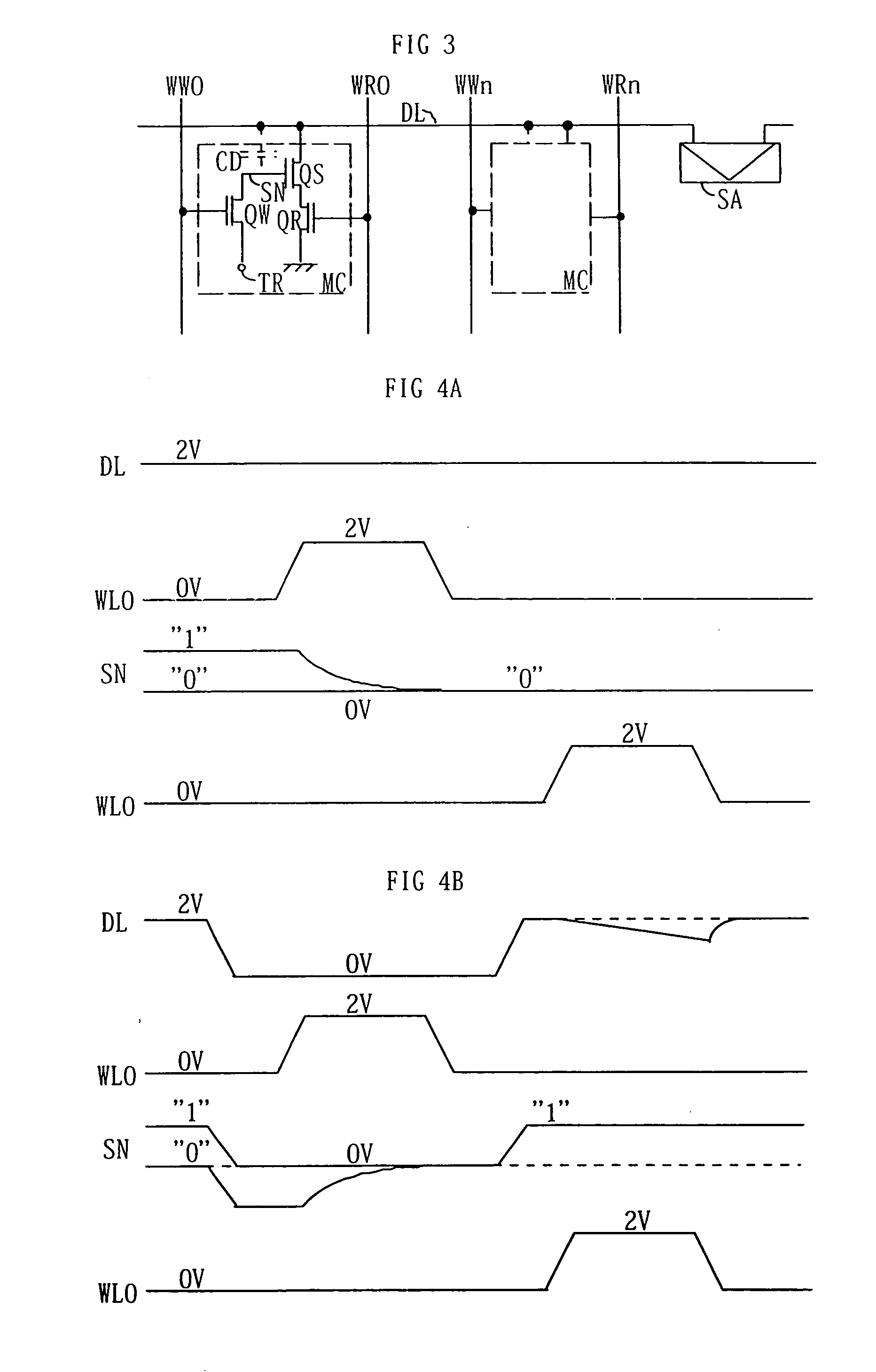
[0098] The memory described in this embodiment preferably incorporates a refresh method divided into two separate cycles. In the first cycle, the data for the row of cells being refreshed is read into a storage register LE. This follows a similar operation as a standard read cycle in the first embodiment except that after the voltage is fully developed in the sense amplifier SA and the output data line DOUT, the data is stored in a register LE through the input TD by the activation of the data store signal at the node TC. In a subsequent cycle, the refresh operation continues with the voltage on the storage node NS being fully restored. During this cycle, the voltage stored in the storage register is presented to the input data DIN and passed to the read data line D0 directly through the activation of the N-channel and P-channel pass transistor pair Q5, Q7. After this data is set on the read data line, the write word line for the row under refresh is activated and deactivated, and t...
third embodiment
[0108] A write operation begins with a similar read data line DR0 and source data line DL0 activation method as described in the third exemplary embodiment. After the read data line DR0 and source data line DL0 are set at appropriate voltages, the word line WL0 is raised to a high voltage that activates the write transistor QW and equalizes the storage node NS with the fixed voltage reference TR. Following word line Wl0 deactivation, the read and source data lines are returned to the standby state, storing a voltage value on the storage node NS. As in the third embodiment, the stored voltage in the high state is Vref+Vr*Cr / Ctot and the voltage of the low state is Vref−Vs*Cs / Ctot. The values are designed such that the low voltage state does not activate the storage transistor QS.
[0109] A read operation is started when the read data line DR0 is floated and the word line WL0 voltage is lowered. The change in voltage induced on the storage node is −Vw*Cw / Ctot. These values are designed ...
PUM
 Abstract
Description
Claims
Application Information