
High-resistance silicon wafer and process for producing the same

a technology of high-resistance silicon and silicon wafer, which is applied in the direction of after-treatment details, transportation and packaging, under a protective fluid, etc., can solve problems such as unrealistic measures, and achieve the effects of preventing reducing unstable resistivity because of the generation of oxygen donors, and reducing unstable resistivity

Active Publication Date: 2005-11-10
SUMCO CORP
View PDF10 Cites 36 Cited by
  • Summary
  • Abstract
  • Description
  • Claims
  • Application Information

AI Technical Summary

Benefits of technology

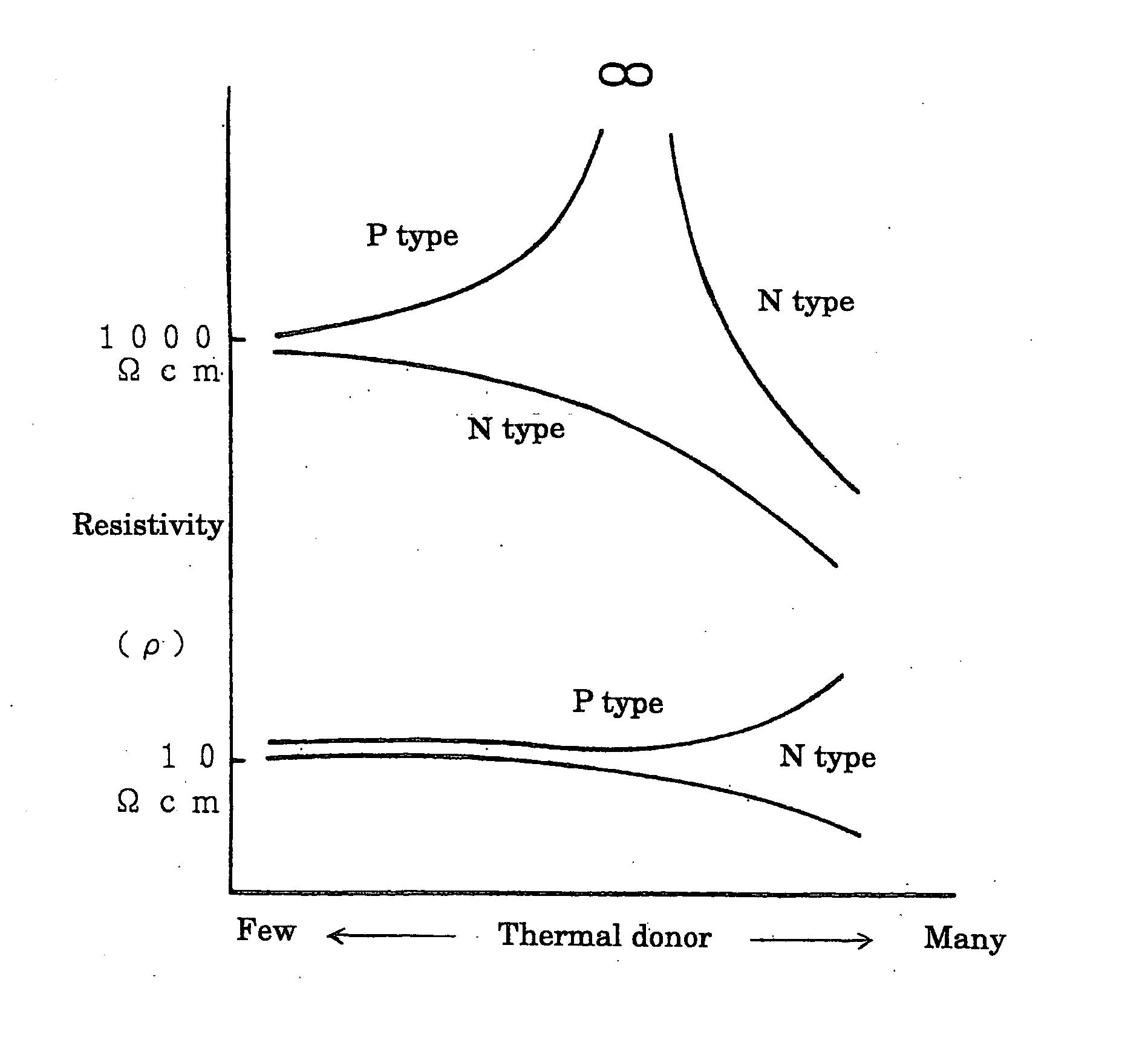
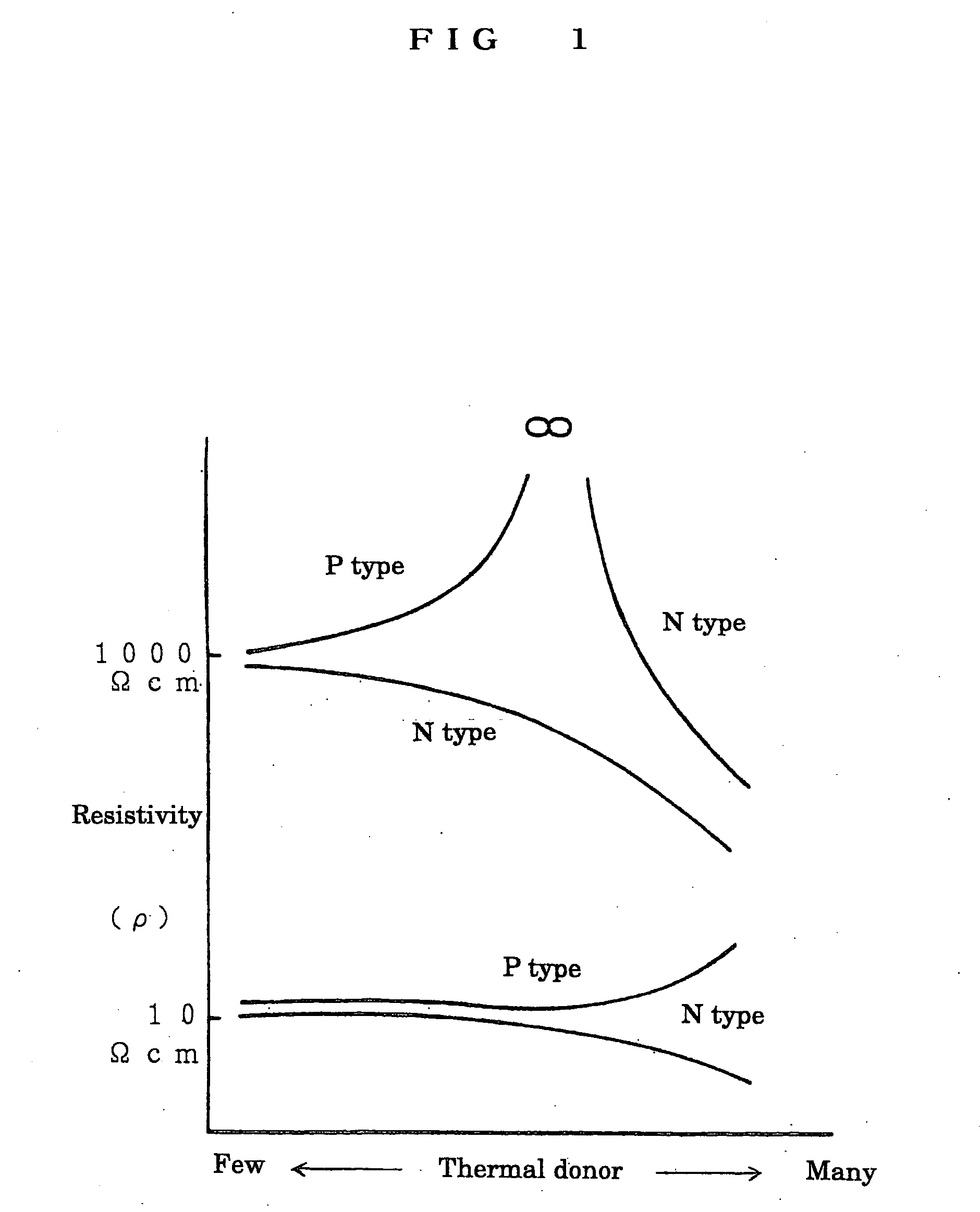
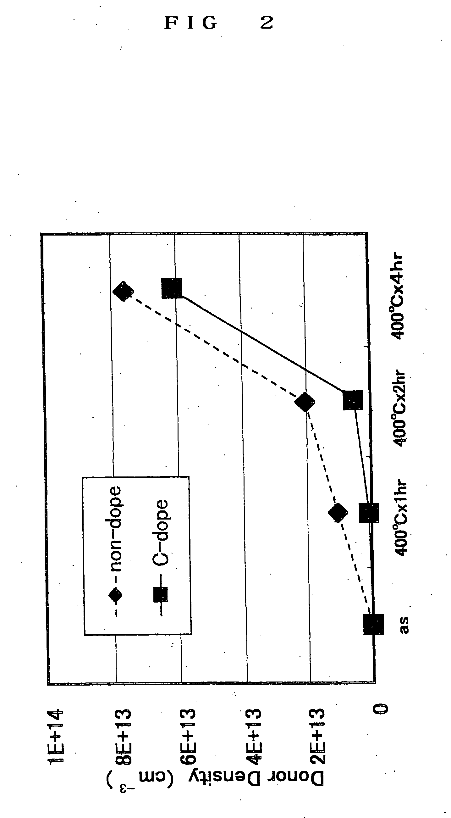
[0014] In order to attain the above objects, the inventors of the present invention have determined that a cause of the above problems lies in the excessive generation of the oxygen precipitate (BMD) and the considerable lowering of the remaining oxygen concentration in the product wafer caused by the excessive generation thereof, and studied about measures for preventing the generation of oxygen donor instead of the generation of the oxygen precipitate (BMD) in the high-resistance silicon wafer. As a result, they discovered that carbon doping is effective in preventing generation of the oxygen donor, especially in preventing generation of the thermal donor, and when a heat treatment is performed in addition to the carbon doping, the generation of the oxygen donor such as the thermal donor and a new donor is more effectively prevented, and many existing heat treatments which are generally used in a process of manufacturing various kinds of wafers such as a DZ wafer, a hydrogen annealed wafer, a SIMOX type and a bonded type of SOI wafer can be used as the heat treatment which is effective in preventing the generation of the oxygen donor.

Problems solved by technology

Since such carbon doping at high concentration accelerates dislocation in the growth of the single crystal by the CZ method and its crystallization becomes difficult, it is not realistic measures.

Method used


Image

  • High-resistance silicon wafer and process for producing the same
  • High-resistance silicon wafer and process for producing the same
  • High-resistance silicon wafer and process for producing the same

Examples


first embodiment

( DZ Wafer)

[0058] As the first step, a high-oxygen, high-resistance and carbon-doped silicon single crystal is formed by a normal CZ method. As the second step, a primary substrate in which for example, an amount of oxygen is 10 to 18×1017 atoms / cm3, an amount of carbon is 5×10¹⁵ to 5×10¹⁷ atoms / cm3 and resistance is high (100 Ωcm or more) is formed from the silicon single crystal.

[0059] As the third step, an OD treatment is performed on the primary substrate at 1100 to 1200° C. for 1 to 4 hours. By this OD treatment, an oxygen precipitate (BMD) is prevented from being generated in the vicinity of a wafer surface in the heat treatment as will be described below. Thus, a DZ (Denuded Zone) layer is formed at least 5 μm or more in depth from a surface of a product wafer.

[0060] The OD treatment can be performed in an atmosphere of a mixed gas of nitrogen gas and oxygen gas. In addition, it can be performed in a hydrogen gas atmosphere. Furthermore, it can be performed in argon gas atm...

second embodiment

( Epitaxial Wafer)

[0066] As the first step, a high-oxygen, high-resistance and carbon-doped silicon single crystal is formed by a normal CZ method. As the second step, a primary substrate in which for example, an amount of oxygen is 10 to 18×1017 atoms / cm3 or more, an amount of carbon is 5×10¹⁵ to 5×10¹⁷ atoms / cm3 and resistance is high (100 Ωcm or more) is formed from the silicon single crystal.

[0067] As the third step, an OD treatment is performed on the primary substrate at 1100 to 1200° C. for 1 to 4 hours. As the fourth step, a heat treatment for forming an oxygen precipitate nucleus is performed under a condition of at 550 to 950° C. for 1 hour or more. As the fifth step, a heat treatment is performed at 900 to 1100° C. for 1 hour or more as a heat treatment for forming a nucleus of the oxygen precipitate and as a heat treatment for growing the oxygen precipitate.

[0068] As the sixth step, after a hydrogen baking process at about 1180° C. is performed on each substrate proces...

third embodiment

( SIMOX Wafer)

[0076] As the first step, a high-oxygen, high-resistance and carbon-doped silicon single crystal is formed by a normal CZ method. As the second step, a primary substrate in which for example, an amount of oxygen is 10 to 18×1017 atoms / cm3 or more, an amount of carbon is 5×10¹⁵ to 5×10¹⁷ atoms / cm3 and resistance is high (100 Ωcm or more) is formed from the silicon single crystal.

[0077] As the third step, oxygen ions are accelerated to 30 to 200 keV and ion injection is performed in a surface of the primary substrate at a density of about 1018 atoms / cm3. As the fourth step, a heat treatment is performed on the substrate provided at the third step at 1250 to 1400° C. for 1 to 20 hours in an atmosphere of oxygen gas or argon gas or mixed oxygen and argon gas, to form a BOX layer (buried oxide film layer) in the substrate.

[0078] The SIMOX wafer product as thus manufactured has following characteristics.

[0079] Since a general-purpose silicon wafer having a relatively high...


PUM


Abstract

A high-resistance silicon wafer is manufactured, in which a gettering ability and economical efficiency is excellent and an oxygen thermal donor is effectively prevented from being generated in a heat treatment for forming a circuit, which is to be implemented on the side of a device manufacturer. In order to implement the above, a high-temperature heat treatment at 1100° C. or higher is performed on a carbon doped high-resistance and high-oxygen silicon wafer in which specific resistivity is 100 Ωcm or more and a carbon concentration is 5×10¹⁵ to 5×10¹⁷ atoms / cm3 so that a remaining oxygen concentration becomes 6.5×10¹⁷ atoms / cm3 or more (Old-ASTM). As this high-temperature treatment, an OD treatment for forming a DZ layer on a wafer surface, a high-temperature annealing treatment for eliminating a COP on the surface layer, a high-temperature heat treatment for forming a BOX layer in a SIMOX wafer manufacturing process and the like can be used.

Description

TECHNICAL FIELD [0001] The present invention relates to a high-resistance silicon wafer used in a support substrate and the like in a high-frequency communication device or an analog-digital device and its manufacturing method. BACKGROUND ART [0002] Recently, a demand for high-resistance substrate is increased along with the widespread use of a high-frequency communication device used in a short-distance wireless LAN. Conventionally, a compound semiconductor substrate such as GaAs has been mainly used as a support substrate of a RF (Radio Frequency: high frequency) circuit which requires high resistance. However, the compound semiconductor substrate is very expensive. [0003] Meanwhile, a silicon CMOS requires a large amount of power, so that it has been considered that it is not suitable for the RF circuit. However, because of recent considerable miniaturization and development of designing, it can be applied to the RF circuit. Therefore, a high-resistance silicon wafer which is exc...

Claims


Application Information

Patent Timeline
IPC IPC(8): C30B29/06C30B33/00H01L21/322H01L21/762
CPCC30B29/06C30B33/00Y10T428/21H01L21/76243H01L21/3225
Inventor SADAMITSU, SHINSUKETAKASE, NOBUMITSUTAKAO, HIROYUKISUEOKA, KOJIHORAI, MASATAKA
Owner SUMCO CORP
Learn More