
Support for hybrid epitaxy and method of fabrication

Inactive Publication Date: 2005-12-08
S O I TEC SILICON ON INSULATOR THECHNOLOGIES
View PDF6 Cites 68 Cited by
  • Summary
  • Abstract
  • Description
  • Claims
  • Application Information

AI Technical Summary

Benefits of technology

[0027] Thus, the cost of producing a support for epitaxy is significantly reduced by forming a layer of monocrystalline SiC in a substrate of conducting SiC. In fact, the cost of a conducting SiC substrate is 5 times lower than that of a semi-insulating SiC substrate.
[0028] Further, in the case of GaN, forming a semi-insulating layer of GaN in a conducting GaN substrate can produce GaN substrates with electrical conductivity that is compatible with high frequency power applications, which is impossible with GaN as currently available in bulk form.
[0030] Another embodiment of the invention relates to a method for facilitating epitaxial growth of a layer of a nitride material, which comprises providing a layer of an insulating monocrystalline carbide or nitride on a substrate formed from a polycrystalline ceramic material having thermal conductivity of at least 1.5 W.cm−1.K−1 so that the nitride layer can be epitaxially grown thereon. If desired, an active conducting layer can be formed on the epitaxially grown layer, and the active layer can be etched or otherwise processed to form at least one electronic component, such as an inductor, capacitor, transmission line, or transistor.

Problems solved by technology

In fact, the cost of a conducting SiC substrate is 5 times lower than that of a semi-insulating SiC substrate.
Further, in the case of GaN, forming a semi-insulating layer of GaN in a conducting GaN substrate can produce GaN substrates with electrical conductivity that is compatible with high frequency power applications, which is impossible with GaN as currently available in bulk form.

Method used


Image

  • Support for hybrid epitaxy and method of fabrication
  • Support for hybrid epitaxy and method of fabrication
  • Support for hybrid epitaxy and method of fabrication

Examples


Embodiment Construction

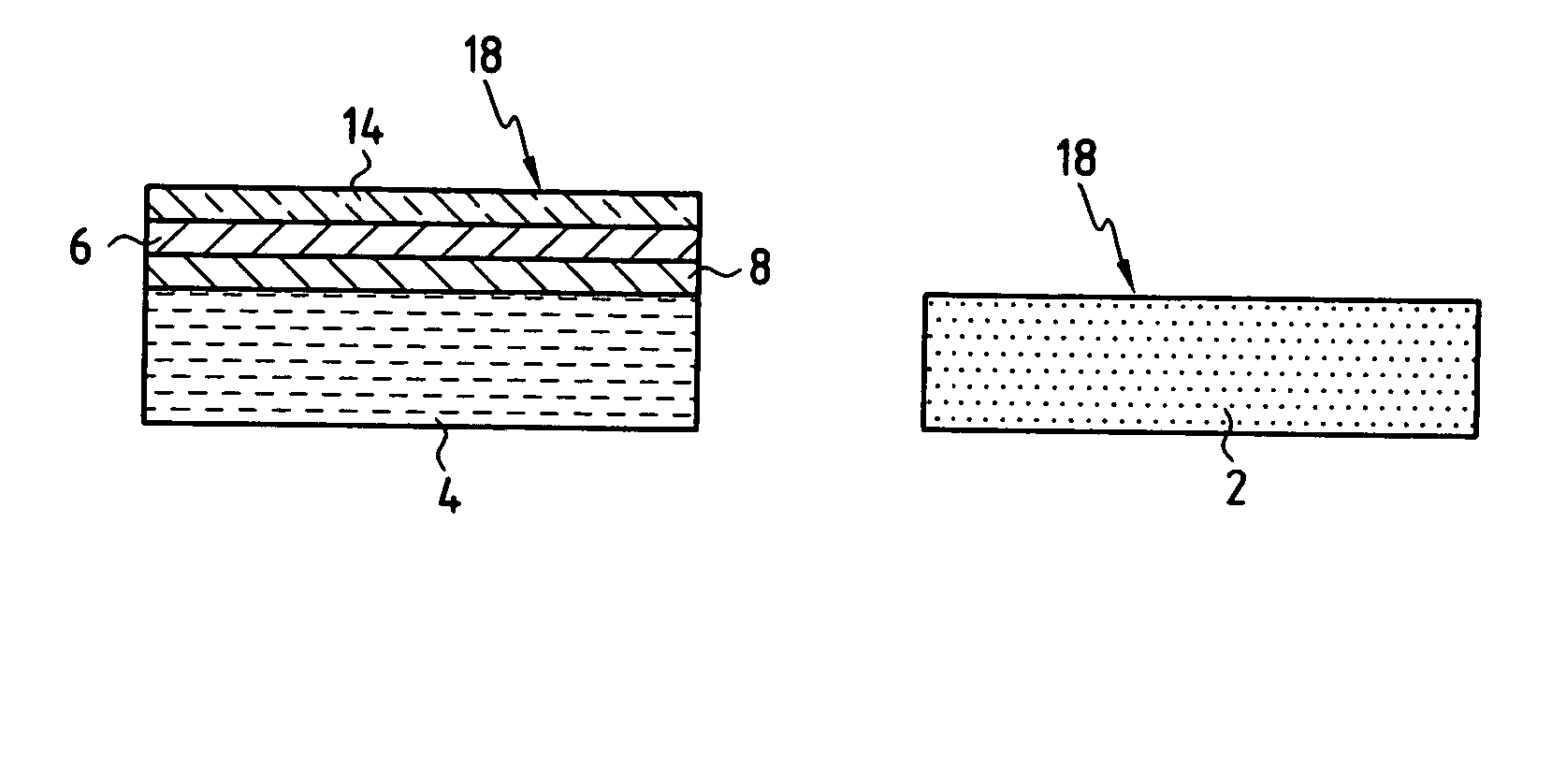
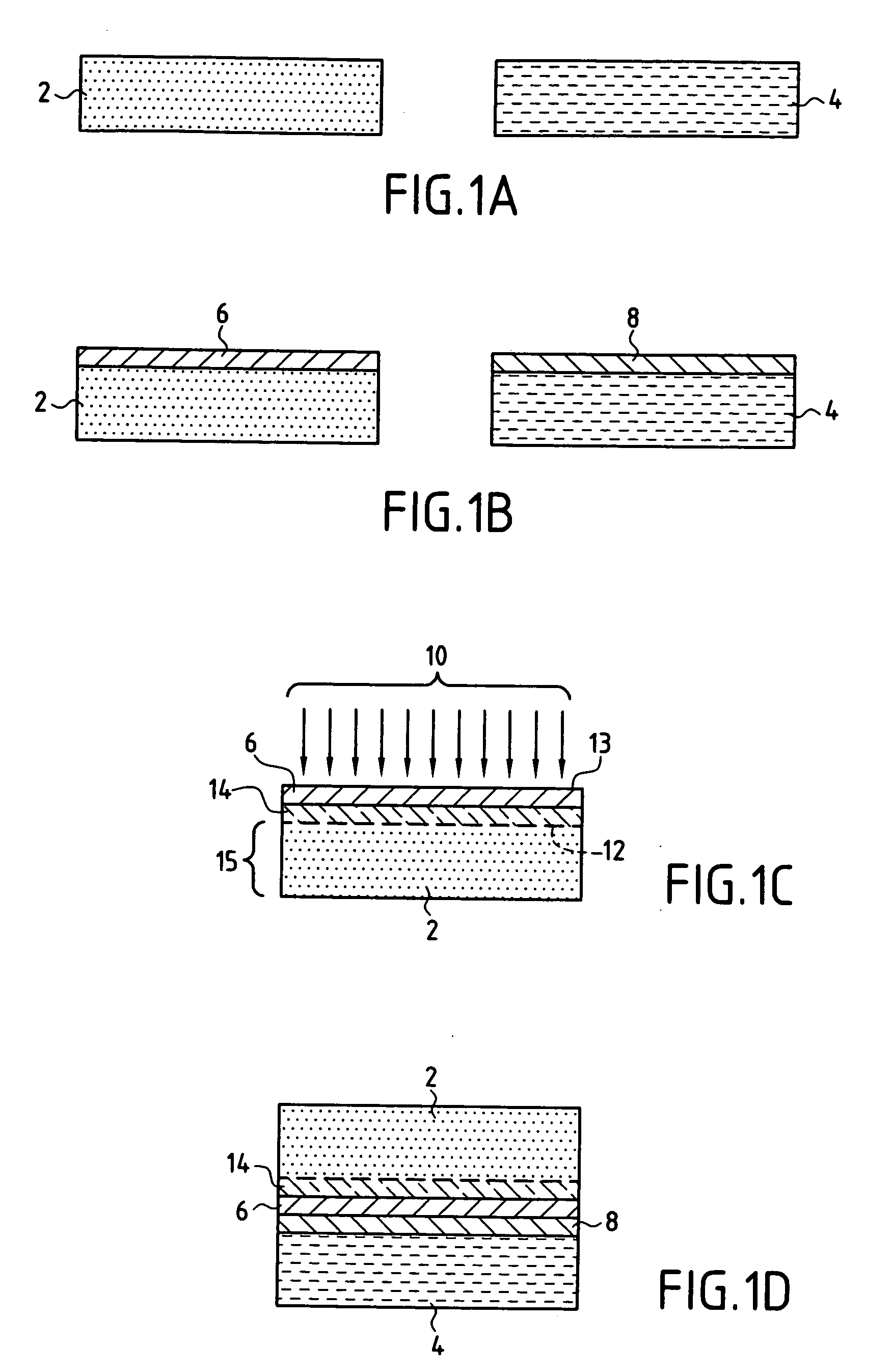
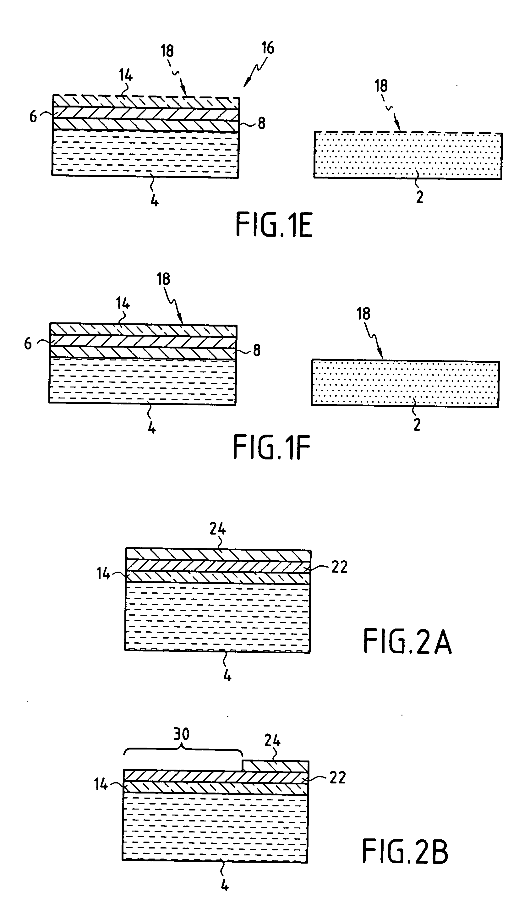
[0034] In a particular implementation, the layer of monocrystalline SiC or GaN can preferably be produced by ion implantation of hydrogen or a rare gas such as helium or argon, or a hydrogen / rare gas combination (co-implantation) into the first conducting monocrystalline SiC or conducting monocrystalline GaN substrate. This implementation has the advantage that the initially conducting SiC or GaN becomes insulating or semi-insulating after implantation, regardless of the SiC polytype used initially for the first substrate. This property of high resistivity of the film after transfer by implantation followed by high temperature annealing persists even after annealing for several hours at 1300° C. This high resistivity of the transferred thin film will thus be conserved after epitaxy of a nitride (GaN, AlN, InN or compounds thereof).

[0035] The second substrate onto which the insulating monocrystalline SiC layer is transferred can be a polycrystalline SiC having electrical resistivity...


PUM

PropertyMeasurementUnit
Temperatureaaaaaaaaaa

Abstract

A method for producing a support for epitaxy by forming a layer of insulating monocrystalline silicon carbide or insulating monocrystalline gallium nitride in a first substrate of conducting monocrystalline silicon carbide or gallium nitride. The method also includes transfer of the monocrystalline layer of silicon carbide or gallium nitride onto a second substrate formed from a polycrystalline ceramic material having thermal conductivity of 1.5 W.cm−1.K−1 or more. This method enables high performance electronic components to be produced cheaply, in particular for high frequency power applications.

Description

FIELD OF THE INVENTION AND BACKGROUND ART [0001] The invention relates to the field of techniques for epitaxy, in particular for the production of layers of materials such as gallium nitride (GaN), aluminum nitride (AlN), indium nitride (InN), or their compounds. [0002] It also relates to the field of radio frequency (RF) and microwave circuits based on materials such as GaN, AlN and their compounds. [0003] As yet, there is still no method for pulling an ingot to produce monocrystalline substrates of GaN or other nitrides that is similar to the method of pulling silicon. Such materials are primarily obtained by forming a thin film by hetero-epitaxy on substrates that are essentially formed from sapphire (Al2O3), but are also in some cases formed from silicon carbide (SiC) or silicon (Si). Although nitrides are usually used in the form of a thin film, it is also possible to find monocrystalline GaN in the form of a bulk material. Such substrates are obtained by hetero-epitaxy of a th...

Claims


Application Information

Patent Timeline
IPC IPC(8): C30B33/00H01L21/20H01L21/335H01L21/762H01L29/20H01L29/778
CPCC30B29/36C30B29/403C30B29/406H01L29/7787H01L21/76254H01L29/2003H01L29/66462C30B33/00
Inventor FAURE, BRUCELAHRECHE, HACENE
Owner S O I TEC SILICON ON INSULATOR THECHNOLOGIES
Learn More