Method and apparatus for linear low-frequency feedback in monolithic low-noise charge amplifiers

a low-noise charge amplifier and low-frequency feedback technology, applied in the direction of charge amplifiers, amplifier combinations, positive-feedback circuit arrangements, etc., can solve the problems of feedback instability, difficult to implement high-value resistors using conventional complimentary metal oxide semiconductor (cmos) fabrication methods, periods of inoperability, etc., to minimize the number of components and maximize the dynamic range

Active Publication Date: 2005-12-15
BROOKHAVEN SCI ASSOCS
View PDF5 Cites 5 Cited by
  • Summary
  • Abstract
  • Description
  • Claims
  • Application Information

AI Technical Summary

Benefits of technology

[0030] It is an object of the present invention to provide a charge sensitive amplifier with a stable, high-resistance feedback circuit, which maximizes dynamic range at its output while minimizing the number of components.

Problems solved by technology

However, high-value resistors are difficult to implement using conventional complimentary metal oxide semiconductor (CMOS) fabrication methods.
These configurations suffer from several disadvantages, such as periods of inoperability, feedback instability, and very large variations in the resistance of the feedback element due to variations in process, temperature, and power supply voltage.
The major drawbacks include non-linearity, noise contributions, and a voltage drop limiting the dynamic range available at the output of the amplifier.
These problems become even more critical as the supply voltage and metal oxide semiconductor field effect transistor (MOSFET) threshold voltage decrease.
However, this solution becomes substantially more difficult to use with more recent CMOS technologies of 0.25 μm or less, which need to be operated at supply voltages of 2.5 volts or less.
One of the problems with such circuits concerns discharging the preamplifier feedback capacitor C4.
However, with complementary metal oxide semiconductor (CMOS) technology, realistic values can only be provided in the range of tens of kilohms.
However, the configuration shown in FIG. 4 is non-linear, that is, due to the low mirror current and voltage mismatches, pole-zero cancellation is fully effective only when C4 equals C5.
In addition, this configuration is noisy, that is, resistor R2 and MOSFETs in the current mirror 22 contribute substantially to the noise generated by the feedback network.
However, like the configuration shown in FIG. 2, the amplifier in FIG. 5 is non-linear due to the lack of pole-zero cancellation.
In addition, this configuration is not self-adaptive to the sensor leakage current, that is, the maximum leakage current that can be absorbed by the circuit is equal to the tail current of the differential pair represented by MOSFETs M7, M8.
Leakage currents greater than this value cannot be absorbed and the configuration exhibits excessive noise for detectors exhibiting leakage currents that are smaller than this value.
Thus, each of the conventional charge sensitive amplifier configurations discussed above suffers from at least one of the three major disadvantages associated with active devices in a feedback network.
These disadvantages being non-linearity, noise, and the dynamic range available at the output of the amplifier.

Method used


Image

  • Method and apparatus for linear low-frequency feedback in monolithic low-noise charge amplifiers
  • Method and apparatus for linear low-frequency feedback in monolithic low-noise charge amplifiers
  • Method and apparatus for linear low-frequency feedback in monolithic low-noise charge amplifiers

Examples


Embodiment Construction

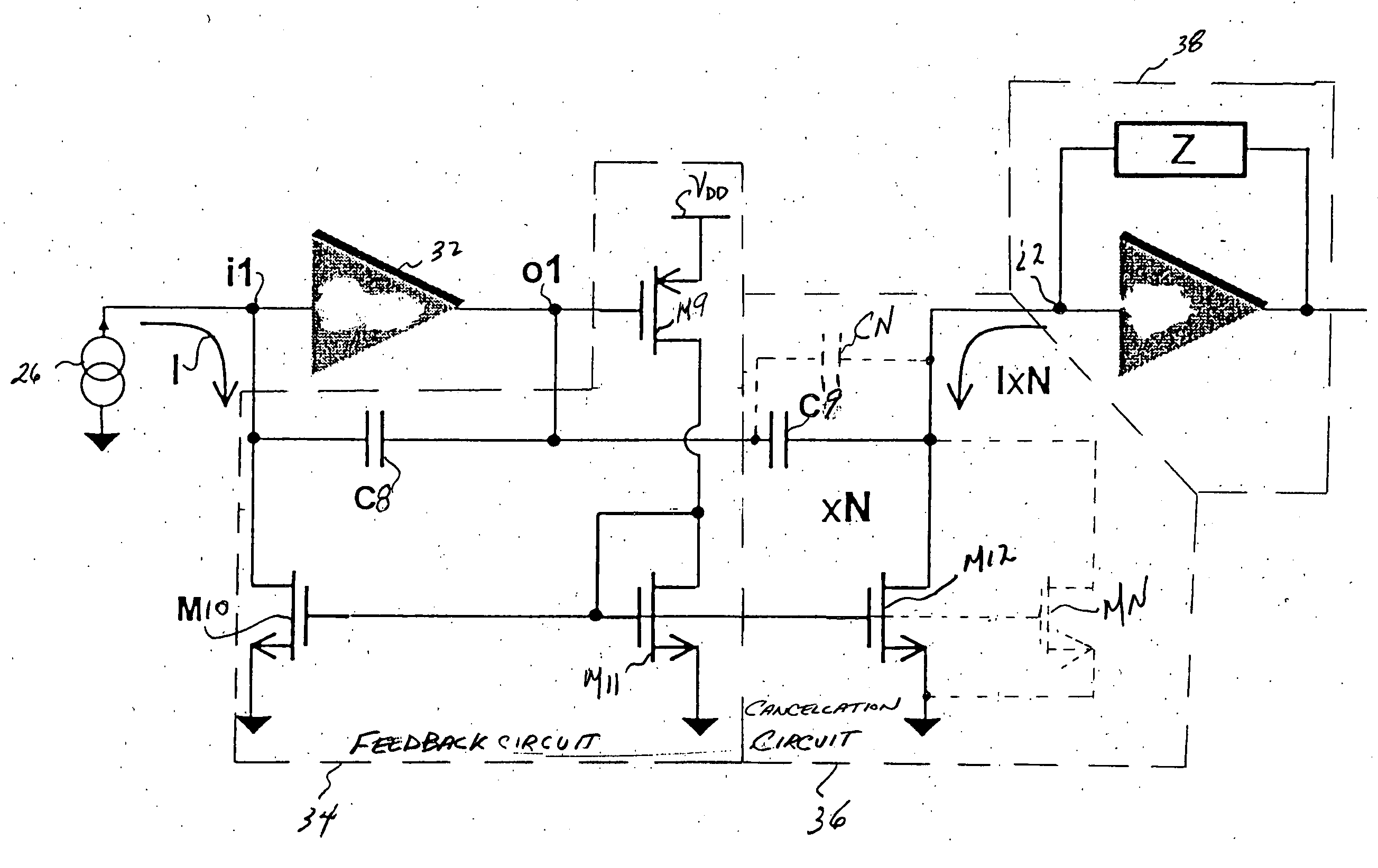
[0056]FIG. 6 shows a block diagram of a charge sensitive amplifier formed in accordance with the present invention, which includes an n-channel metal oxide semiconductor field effect transistor (MOSFET)-based signal amplifier 32 having an input terminal coupled to a current supply 26. A feedback circuit 34 is preferably coupled in parallel across the input and output terminals of the signal amplifier 32. A pole-zero cancellation circuit 36 is preferably coupled in series between the output terminal of the signal amplifier 32 and a second stage amplification circuit 38.

[0057]FIG. 7 shows a more detailed schematic representation of the charge sensitive amplifier shown in FIG. 6. For purposes of illustration, either n-channel MOSFETs or p-channel MOSFETs have been shown herein. However, it is to be understood that transistors of any type may be used, with modifications to the respective circuit that are well known in the art, while remaining within the scope of the present invention. ...


PUM


Abstract

A charge amplifier includes an amplifier, feedback circuit, and cancellation circuit. The feedback circuit includes a capacitor, inverter, and current mirror. The capacitor is coupled across the signal amplifier, the inverter is coupled to the output of the signal amplifier, and the current mirror is coupled to the input of the signal amplifier. The cancellation circuit is coupled to the output of the signal amplifier. A method of charge amplification includes providing a signal amplifier; coupling a first capacitor 10 across the signal amplifier; coupling an inverter to the output of the signal amplifier; coupling a current mirror to the input of the signal amplifier; and coupling a cancellation circuit to the output of the signal amplifier. A front-end system for use with radiation sensors includes a charge amplifier and a current amplifier, shaping amplifier, baseline stabilizer, discriminator, peak detector, timing detector, and logic circuit coupled to the charge amplifier.

Description

[0001] This invention was made with Government support under contract number DE-AC02-98CH10886, awarded by the U.S. Department of Energy. The Government has certain rights in the invention.BACKGROUND OF THE INVENTION [0002] 1. Field of the Invention [0003] The present invention relates to charge sensitive amplifiers, and more particularly relates to a charge sensitive amplifier for use on monolithic substrates, which includes a low-noise, active feedback element that exhibits improved linearity and dynamic range. [0004] 2. Description of the Prior Art [0005] Charge sensitive amplifiers are used in a variety of commercial, industrial, medical, and scientific instrumentation applications where a signal from a sensor is provided in the form of a small current charge that requires amplification prior to further signal processing or conditioning. These sensors may include low-capacitance silicon detectors, such as those used in particle position sensing, X-ray spectroscopy, and X-ray ima...

Claims


Application Information

Patent Timeline
Patent Type & Authority Applications(United States)
IPC IPC(8): H03F1/36H03F1/34H03F3/70
CPCH03F1/34H03F1/36H03F3/70
Inventor DEGERONIMO, GIANLUIGI
Owner BROOKHAVEN SCI ASSOCS
Why Eureka
Try Eureka