Method and apparatus for producing large, single-crystals of aluminum nitride

a technology of aluminum nitride and single crystals, which is applied in the direction of crystal growth process, polycrystalline material growth, chemically reactive gas, etc., can solve the problems of high production cost, high production cost, and gan epitaxy is far from being an ideal substrate for apphir

Inactive Publication Date: 2006-01-12
CRYSTAL
View PDF32 Cites 53 Cited by
  • Summary
  • Abstract
  • Description
  • Claims
  • Application Information

AI Technical Summary

Problems solved by technology

However, sapphire is far from being an ideal substrate for GaN epitaxy.
Its lattice mismatch to GaN is large (about 16%), it has little distinction between the + and − directions which can give rise to ± c-axis domains in epitaxial films of GaN, and its differential thermal expansion can lead to cracking during the cooling process after the device fabrication process.
Using sapphire substrates leads to a costly fabrication process since it requires growing buffer layers and using Lateral Epitaxial Overgrowth techniques (LEO).
Even though this announcement is very promising, Nichia's lasers still have problems.
Sapphire, with a very low thermal conductivity, traps that heat, a fault that may trigger burnout down the road.
However, this alternative may increase fabrication cost.
However, 2H SiC (to match the 2H crystal structure of GaN) is not available and the lattice mismatch along the c-axis between GaN and both 4H and 6H SiC is substantial.
In addition, the chemical bonding between the Group IV elements of the SiC and the Group-III or Group-V elements of the nitrides is expected to create potential nucleation problems leading to electronic states at the interface.
While this possibility has become more attractive in the last few years, it does not appear to be commercially feasible to fabricate large bulk crystals of GaN in the short term.
Unfortunately, however, most attempts at increasing the growth rate of AlN crystals under such stoichiometric and / or sub atmospheric pressure conditions have met with limited success.
In addition, it appears to be impossible to achieve the growth rate, or the electronics-grade quality Hunter discloses in his patents with the nitrogen pressure below one atmosphere.
Disadvantageously, it would be difficult to grow large boules of AlN this way since: (i) control of growth would be difficult (since it would be non-uniform across the surface), (ii) a large amount of Al would be wasted, (iii) the excess Al in the rest of the furnace would create problems because of its high reactivity, and (iv) it would be difficult to maintain high differences in temperature (Δ T) between the source and growing crystal surface.

Method used


Image

  • Method and apparatus for producing large, single-crystals of aluminum nitride
  • Method and apparatus for producing large, single-crystals of aluminum nitride
  • Method and apparatus for producing large, single-crystals of aluminum nitride

Examples


example — 260

Example—260 nm Laser Diode Fabrication

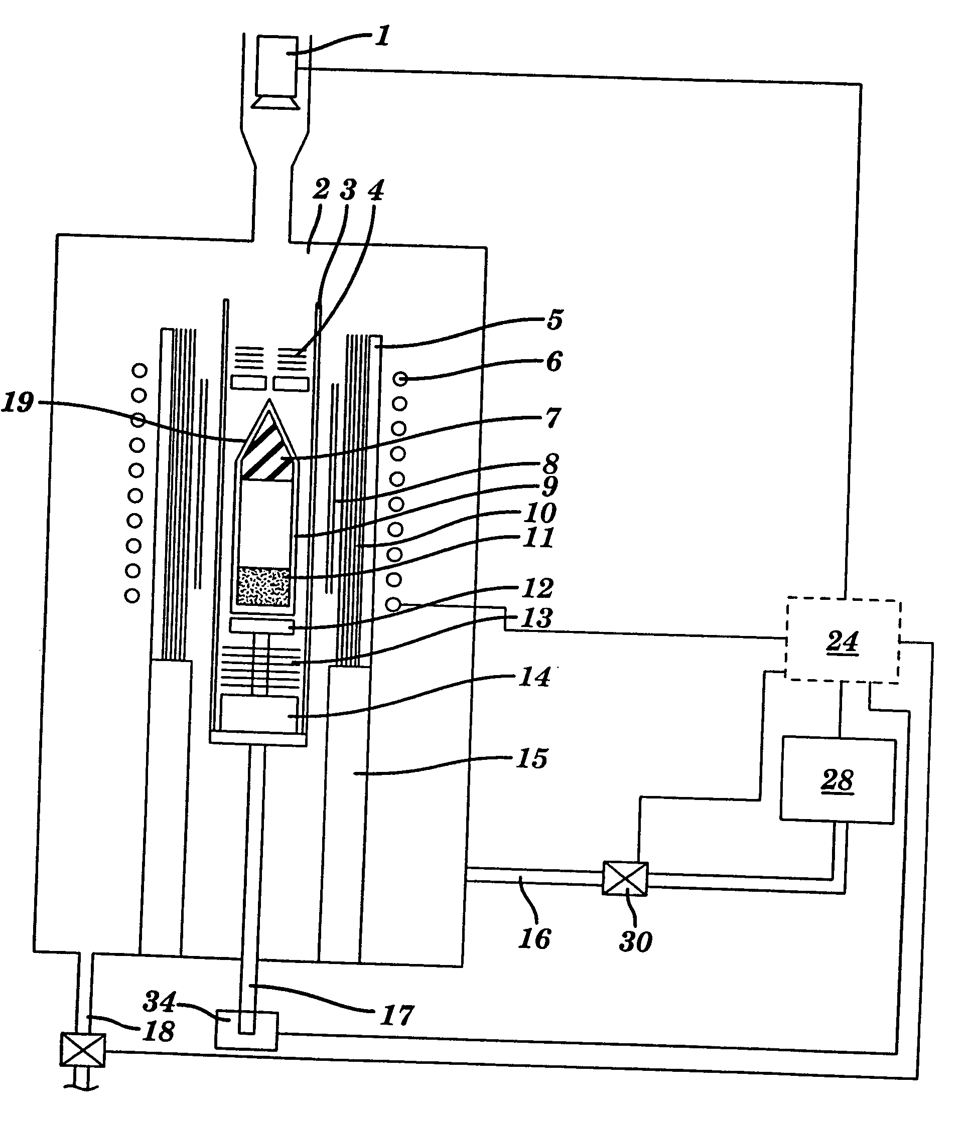
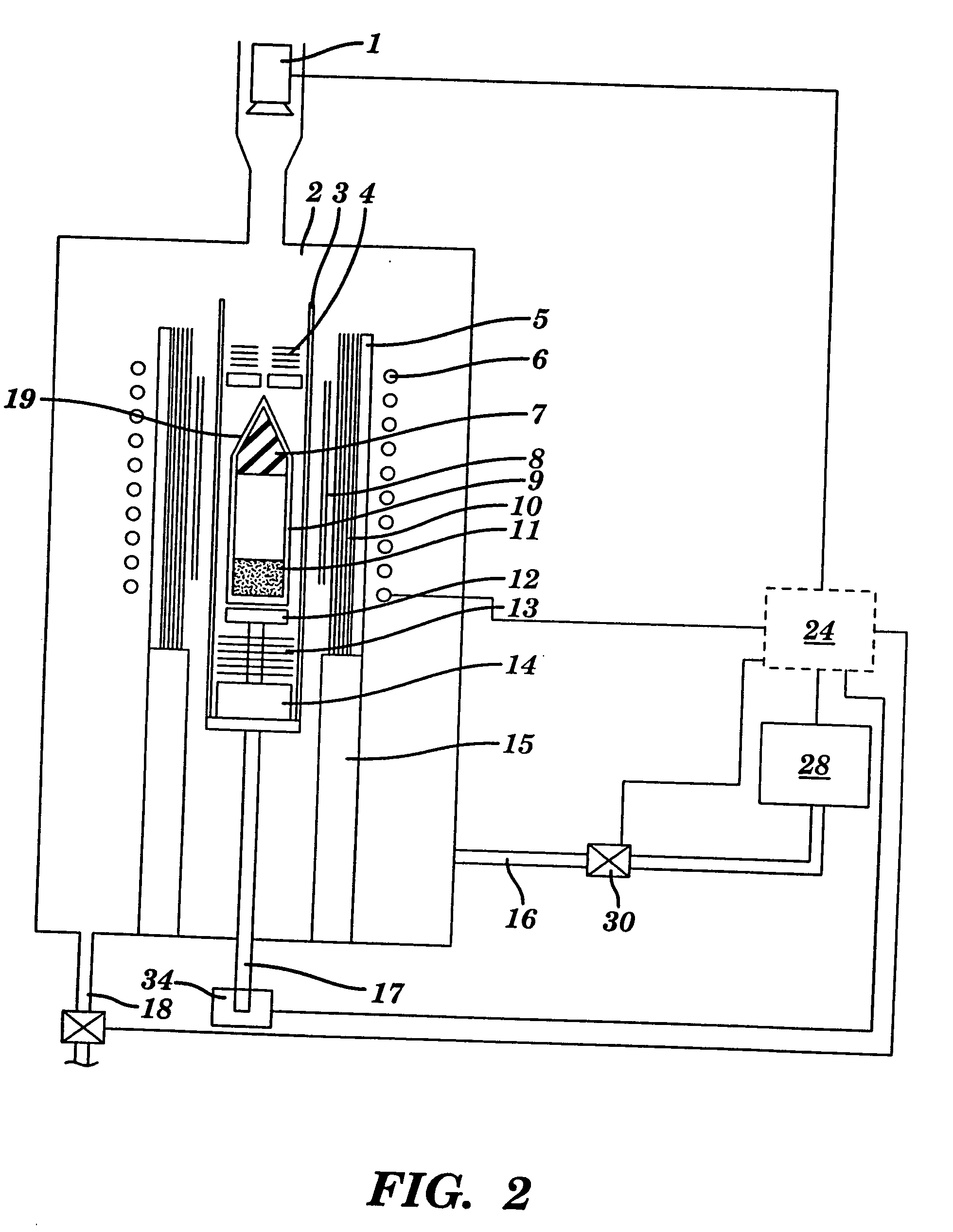
[0080]FIG. 6 is a schematic cross-sectional view of a portion of a 260 nm laser diode fabricated using the method of the present invention. Initially, low defect density AlN substrate 40, which is prepared using the method discussed above, is polished by chemical mechanical polishing (CMP). Polished substrate 40 is then introduced into a conventional organo-metallic vapor phase epitaxy system (OMVPE). The surface of the low defect density AlN substrate is cleaned to remove any oxide or other impurities on the crystal surface. Cleaning is effected by heating the substrate at a temperature of 1150° C. for 20 min under ammonia plus nitrogen or hydrogen plus nitrogen flow prior to growth. An epitaxial layer 42 of AlN having a thickness of about 100 nm is then grown on substrate 40 to improve the surface quality of AlN substrate 40 before starting to grow the device layers. Next an undoped AlxGa1-xN buffer layer 44 having a thickness of approximately...


PUM

PropertyMeasurementUnit
temperatureaaaaaaaaaa
wavelengthsaaaaaaaaaa

Abstract

A method and apparatus for producing bulk single crystals of AlN having low dislocation densities of about 10,000 cm−2 or less includes a crystal growth enclosure with Al and N2 source material therein, capable of forming bulk crystals. The apparatus maintains the N2 partial pressure at greater than stoichiometric pressure relative to the Al within the crystal growth enclosure, while maintaining the total vapor pressure in the crystal growth enclosure at super-atmospheric pressure. At least one nucleation site is provided in the crystal growth enclosure, and provision is made for cooling the nucleation site relative to other locations in the crystal growth enclosure. The Al and N2 vapor is then deposited to grow single crystalline low dislocation density AlN at the nucleation site. High efficiency ultraviolet light emitting diodes and ultraviolet laser diodes are fabricated on low defect density AlN substrates, which are cut from the low dislocation density AlN crystals. Bulk crystals of ZnO may also be produced using the method.

Description

RELATED APPLICATIONS [0001] This application is a continuation-in-part of co-pending U.S. patent application Ser. No. 10 / 324,998 filed Dec. 20, 2003, entitled METHOD FOR PRODUCING LARGE SINGLE-CRYSTALS OF ALUMINUM NITRIDE, now issued as U.S. Pat. No. ______ on ______ and claims the benefit of U.S. Provisional Application Ser. No. 60 / 344,672, entitled METHOD FOR PRODUCING LARGE SINGLE-CRYSTALS OF ALUMINUM NITRIDE, filed Dec. 24, 2001.GOVERNMENT SPONSORSHIP [0002] The U.S. Government may have certain rights in this invention pursuant to SBIR Contract N00014-98-C-0053 awarded by the Office of Naval Research, under SBIR Contract F33615-00-C-5531 awarded by the Air Force Research Laboratory, and under SBIR Contract F33615-00-C-5425 awarded by the Missile Defense Agency.FIELD OF THE INVENTION [0003] The present invention relates to the growth of single-crystal Aluminum Nitride (AlN), and more particularly, to relatively large, single-crystal AlN, which are grown by sublimation-recondensat...

Claims


Application Information

Patent Timeline
Patent Type & Authority Applications(United States)
IPC IPC(8): C30B11/00C30B23/00C30B17/00C30B21/02C30B28/14H01L33/00H01L33/02
CPCC30B11/003C30B23/00C30B29/403H01L33/0075H01L2924/0002H01L33/025H01L2924/00
Inventor SCHOWALTER, LEO J.SLACK, GLEN A.ROJO, J. CARLOS
Owner CRYSTAL
Why Eureka
Try Eureka