Translucent electromagnetic shield film, producing method therefor and emulsifier

a technology of electromagnetic shield and translucent film, which is applied in the direction of instruments, metallic image processing, photomechanical equipment, etc., can solve the problems of affecting the health of operators of such equipment, affecting the operation of electromagnetic shield equipment, and increasing the electromagnetic interference (emi) significantly, and achieves high emi shield ability, high transparency, and easy fine line pattern formation

Inactive Publication Date: 2006-01-12
FUJIFILM CORP +1
View PDF22 Cites 19 Cited by
  • Summary
  • Abstract
  • Description
  • Claims
  • Application Information

AI Technical Summary

Benefits of technology

[0021] The present invention has been made in consideration of such situation, and an object of the invention is to provide a producing method for a translucent electromagnetic shield film having a high EMI shield ability and a high transparency at the same time without a moiré pattern, the method being capable of easily forming a fine line pattern and also capable of mass producing the translucent electromagnetic shield film inexpensively. Another object of the invention is to provide a translucent electromagnetic shield film obtained by the aforementioned producing method. Still another object of the invention is to provide a translucent electromagnetic shield film for a plasma display panel containing the aforementioned translucent electromagnetic shield film, an optical filter for a plasma display panel, and a plasma display panel. Still another object of the invention is to provide an emulsion and a silver halide photosensitive material capable of simply forming a metallic silver portion having a high conductivity, and also to provide conductive silver material, an electrode material and a wiring material obtainable therefrom.

Problems solved by technology

With the recent increase in the utilization of various electric facilities and electronic equipment, electromagnetic interferences (EMI) are increasing significantly.
Such EMI not only induces erroneous operations and troubles on electronic / electric equipment but also is pointed out to cause troubles on the health of operators of such equipment.
In the aforementioned methods, the front side of the display generally becomes opaque and such methods are inadequate for a shielding method for the electromagnetic wave.
It is however associated with a drawback that the mesh has to be manufactured through a number of production steps.
Also because of the use of a copper foil, the obtained mesh is not black but has a copper color, thereby causing a decrease in the image contrast of the display equipment.
However, it has not been known at all to prepare a conductive metallic silver by such method for shielding the electromagnetic wave emitted from the image display face of the display such as CRT or PDP without hindering the image display.
Therefore, in an exposed area where the metallic silver film is not formed, opaque physical development nuclei remain thereby hindering the optical transparency.
Such drawback is serious in case of use as a translucent electromagnetic shield material for a display such as CRT or PDP.
Another drawback is a difficulty in obtaining a high conductivity.
Also there is another drawback that the transparency is deteriorated when a thick silver film is formed in order to obtain a high conductivity.
It is therefore not possible, with the aforementioned methods, to obtain a translucent electromagnetic shield material having satisfactory optical transmission and conductivity suitable for shielding an electromagnetic wave emitting from an image display face of an electronic display equipment.
Also in case of obtaining an electroconductivity through the steps of a development, a physical development and a plating utilizing a commercially available negative photographic film instead of the silver salt diffusion transfer process, the resulting film is insufficient, both in the conductivity and the transparency, for use as a translucent electromagnetic shield material for a CRT or a PDP.
As explained above, the prior electromagnetic shield materials and the producing methods therefor have been associated with drawbacks.
However, since such shield plate is very expensive, a reduction in the production cost is strongly desired.
However, an increase in the aperture rate (a proportion of an area without the fine lines constituting the mesh in the entire area) for improving the optical transmittance reduces the conductivity to deteriorate the electromagnetic shielding effect, and it is very difficult in the prior technology to improve the electroconductivity (electromagnetic shield effect) and the optical transmittance at the same time.

Method used


Image

  • Translucent electromagnetic shield film, producing method therefor and emulsifier
  • Translucent electromagnetic shield film, producing method therefor and emulsifier
  • Translucent electromagnetic shield film, producing method therefor and emulsifier

Examples


example 1

[0217] A polyethylene terephthalate (PET) substrate was coated, in succession from the side of the substrate, with an undercoat layer, an antihalation layer, an emulsion layer and a protective layer. Also a backing layer was coated on a side of the substrate opposite to the emulsion layer, thereby obtaining a sample. In the following, a method of preparation of a coating liquid and a coating amount will be explained for each layer.

(Formation of Undercoat Layer)

[0218] An undercoat layer was formed by coating a coating liquid containing gelatin by 50 mg / m2 and lithium silicate by 150 mg / m2.

(Formation of Antihalation Layer)

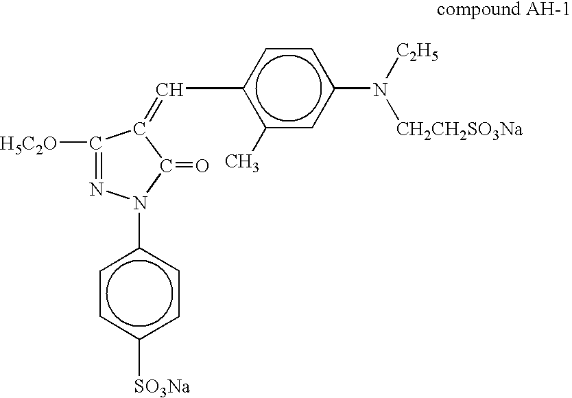
[0219] An antihalation layer was formed by coating a coating liquid containing gelatin by 1 g / m2 and a following compound AH-1 by 150 mg / m2.

(Emulsion Layer)

[0220] An emulsion was prepared in the following manner, corresponding to an emulsion layer of each sample.

* Preparation of Emulsion A

[0221] There was prepared an emulsion A containing 7.5 g of gelati...

example 2

[0275] A silver salt diffusion transfer method for “conductive silver formation utilizing silver salt” described in the related background art and utilizing a silver deposition on a physical development nucleus (for example cf. JP-A No. 2000-149773 and WO01 / 51276) was compared with the samples of the invention, in the following manner.

[0276] On a hydrophilized transparent TAC (triacetyl cellulose) substrate, a physical development nucleus layer and a photosensitive layer were coated, and the sample was then subjected to an exposure through a mesh-shaped photomask of a pitch of 200 μm and a development by a DTR method. Then it was subjected to an electroless silver plating process and an electrolytic Cu plating to obtain a comparative sample C. Also a sample C of the invention was prepared in the same manner as in Example 1, utilizing an emulsion C.

[0277] Both the sample C of the invention and the comparative sample C had a mesh shape of a line width of 12 μm, a pitch of 200 μm and...

example 3

[0281] Samples D and E were prepared with emulsions D and E, in the same manner as in Example 1. Comparative samples An-En were prepared in the same manner as the samples A-E of the invention except that the protective layer was not coated at the preparation of the photosensitive material. These samples were evaluated in the same manner as in Example 1. Also an unevenness in the mesh was evaluated by visual observation under a white transmitting light. The samples of the invention did not show unevenness, while the comparative samples showed unevenness.

TABLE 3Sampledeveloper usedunevennessremarkscomparative sample Andeveloper 2presentcomparativeinvention sample Adeveloper 2absentinventioncomparative sample Bndeveloper 1presentcomparativeinvention sample Bdeveloper 1absentinventioncomparative sample Cndeveloper 1presentcomparativeinvention sample Cdeveloper 1absentinventioncomparative sample Dndeveloper 3presentcomparativeinvention sample Ddeveloper 3absentinvention


PUM

PropertyMeasurementUnit
transparencyaaaaaaaaaa
optical transmittanceaaaaaaaaaa

Abstract

A producing method for a translucent electromagnetic shield film comprising exposing a photosensitive material having an emulsion layer containing a silver salt and a dye on a substrate, then executing a development process to form a metallic silver portion and a light transmitting portion respectively in an exposed area and an unexposed area, and applying a physical development and/or a plating process to the metallic silver portion thereby causing the metallic silver portion to carry a conductive metal. The producing method allows to inexpensively mass produce a translucent electromagnetic shield film without a moiré pattern, having a high EMI shield property and a high transparency at the same time.

Description

BACKGROUND OF THE INVENTION [0001] 1. Field of the Invention [0002] The present invention relates to a producing method for a translucent electromagnetic shield film having transparency and capable of shielding an electromagnetic wave generated from a front face of a display such as a cathode ray tube (CRT), a plasma display panel (PDP), a liquid crystal display, an electroluminescence display (EL) or a field emission display (FED), a microwave oven, an electronic appliance or a printed circuit board, and a translucent electromagnetic shield film obtained by such producing method, also a translucent electromagnetic shield film for a plasma display panel and a plasma display panel having such film. The present invention also relates to a photosensitive silver halide emulsion, a conductive silver film forming material utilizing the same, a silver halide photosensitive material, a conductive silver material and an electrode material. [0003] 2. Background Art [0004] With the recent incr...

Claims


Application Information

Patent Timeline
Patent Type & Authority Applications(United States)
IPC IPC(8): G03C5/00G03C1/005
CPCG03C5/58H05K3/106G03F7/20G03F7/06H05K3/185
Inventor SASAKI, HIROTOMONISHIZAKURA, RYOU
Owner FUJIFILM CORP
Why Eureka
Try Eureka