

Dendritic polymer and electronic device element employing the polymer
a technology of dendrite polymer and electronic device element, which is applied in the direction of non-metal conductors, conductors, synthetic resin layered products, etc., can solve the problems of unsatisfactory characteristics, unsolved service life of organic el devices, and use of pentacene, etc., and achieves high carrier conductivity
- Summary
- Abstract
- Description
- Claims
- Application Information
AI Technical Summary
Benefits of technology
Problems solved by technology
Method used
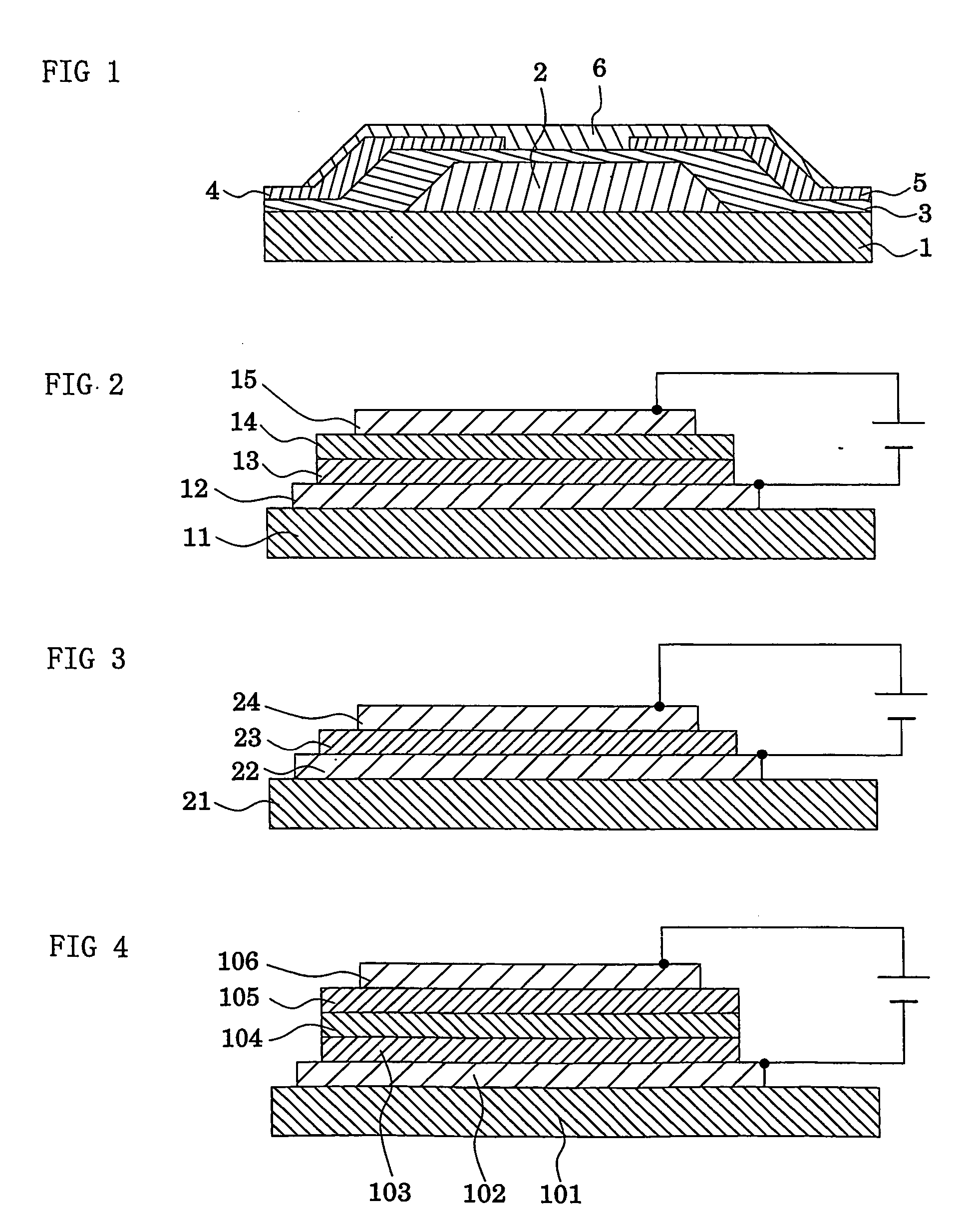
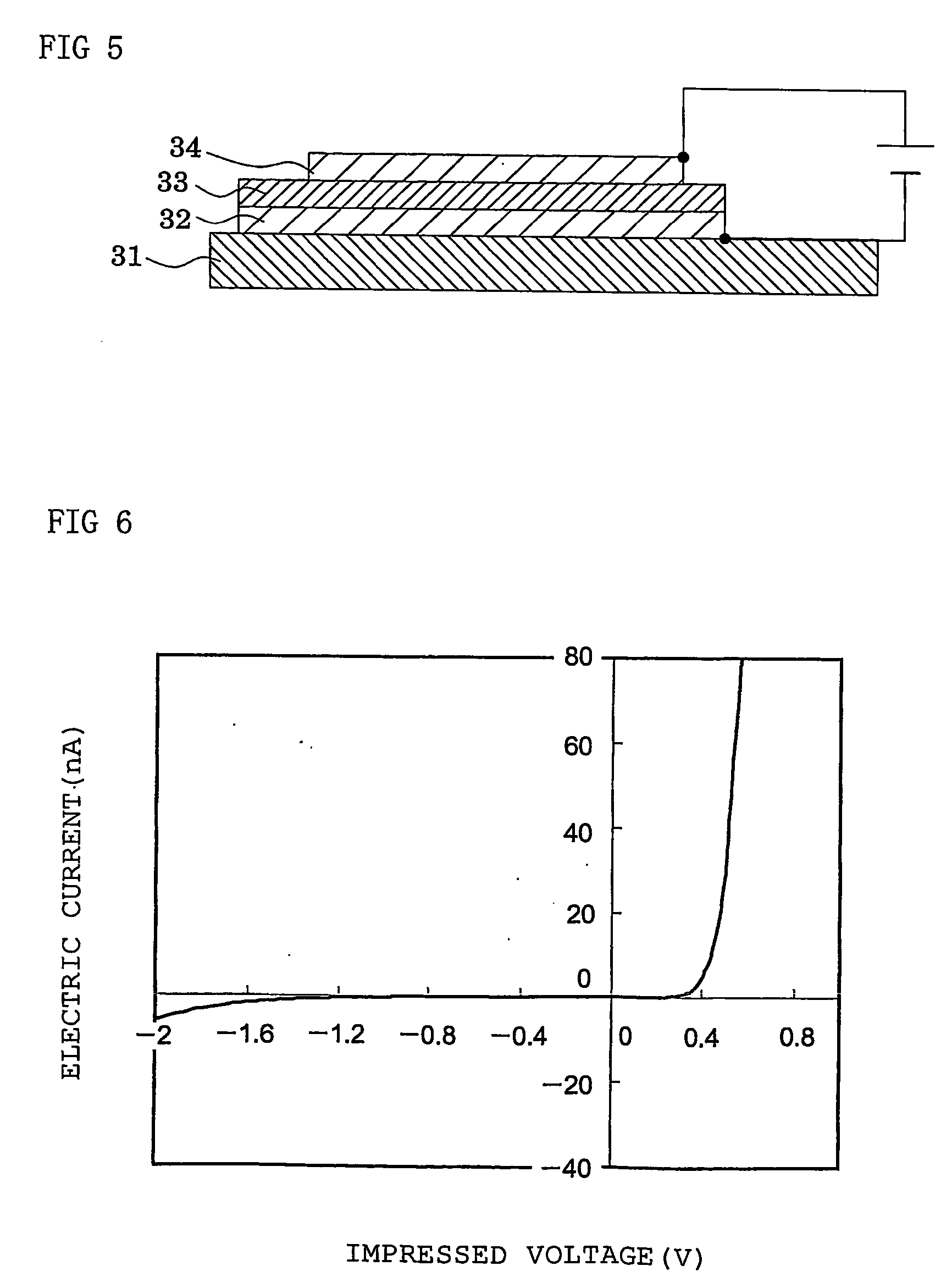
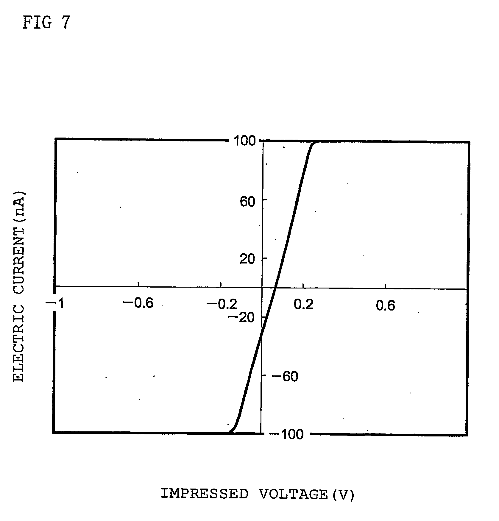
Image

Examples
synthesis example 1
Synthesis of 3rd-Generation Dendritic Polymer
synthesis example 1-1
[0112] Synthesis of a compound (c), 5-(3,5-dibromophenyl)-2,2′-bithiophene, serving as a monomer providing a dendritic structure, represented by the following formula
[0113] In a nitrogen atmosphere, 2,2′-bithiophene (4.6 g) was dissolved in dehydrated tetrahydrofuran, and the solution was cooled in a dry ice—methanol bath. After cooling, a 1.6M n-butyllithium / hexane solution (18 mL) was added dropwise thereto, and the mixture was allowed to react for one hour. Subsequently, trimethoxyborane (3.4 g) was added dropwise thereto, and the resultant mixture was allowed to react for one hour. After completion of reaction, water was added thereto for hydrolysis. Thereafter, the cooling bath was removed, whereby the temperature of the reaction mixture was elevated to room temperature. An aqueous saturated ammonium chloride solution and diethyl ether were added to the reaction mixture, and the resultant mixture was stirred and left to stand. The formed organic layer was isolated from the mi...
synthesis example 1-2
[0118] Synthesis of a compound (a), 5-[2,2′]bithiophenyl-5-yl-N,N,N′,N′-tetraphenyl-1,3-phenylenediamine, forming the branch ends of a dendritic structure, represented by the following formula.
[0119] Xylene (4.5 mL) was added to palladium acetate (10 mg) and, in a nitrogen atmosphere, tri-t-butylphosphine (36 mg) was added thereto. The mixture was heated at 80° C. for 30 minutes, to thereby prepare a catalyst solution.
[0120] Xylene (4.5 mL) was added to a mixture of 5-(3,5-dibromophenyl)-2,2′-bithiophene (1.80 g) which had been produced in Synthesis Example 1-1, diphenylamine (1.60 g) and t-butoxypotassium (1.21 g), and, in a nitrogen atmosphere, the previously prepared catalyst solution was added dropwise thereto at 80° C. After completion of addition, the reaction mixture was heated to 120° C., and was allowed to react for 18 hours. Subsequently, the temperature of the reaction mixture was lowered to room temperature, and water (10 mL) was added thereto. The formed organic laye...
PUM
| Property | Measurement | Unit |
|---|---|---|
| temperature | aaaaa | aaaaa |
| band gap | aaaaa | aaaaa |
| band gap | aaaaa | aaaaa |
Abstract
Description
Claims
Application Information