

Method of manufacturing a semiconductor device
a manufacturing method and semiconductor technology, applied in the direction of semiconductor devices, electrical appliances, transistors, etc., can solve the problems of increasing off, deteriorating reliability, and phenomena becoming large reliability problems, and achieve the effect of reducing light intensity and forming with eas
- Summary
- Abstract
- Description
- Claims
- Application Information
AI Technical Summary
Benefits of technology
Problems solved by technology
Method used
Image

Examples
embodiment mode 1
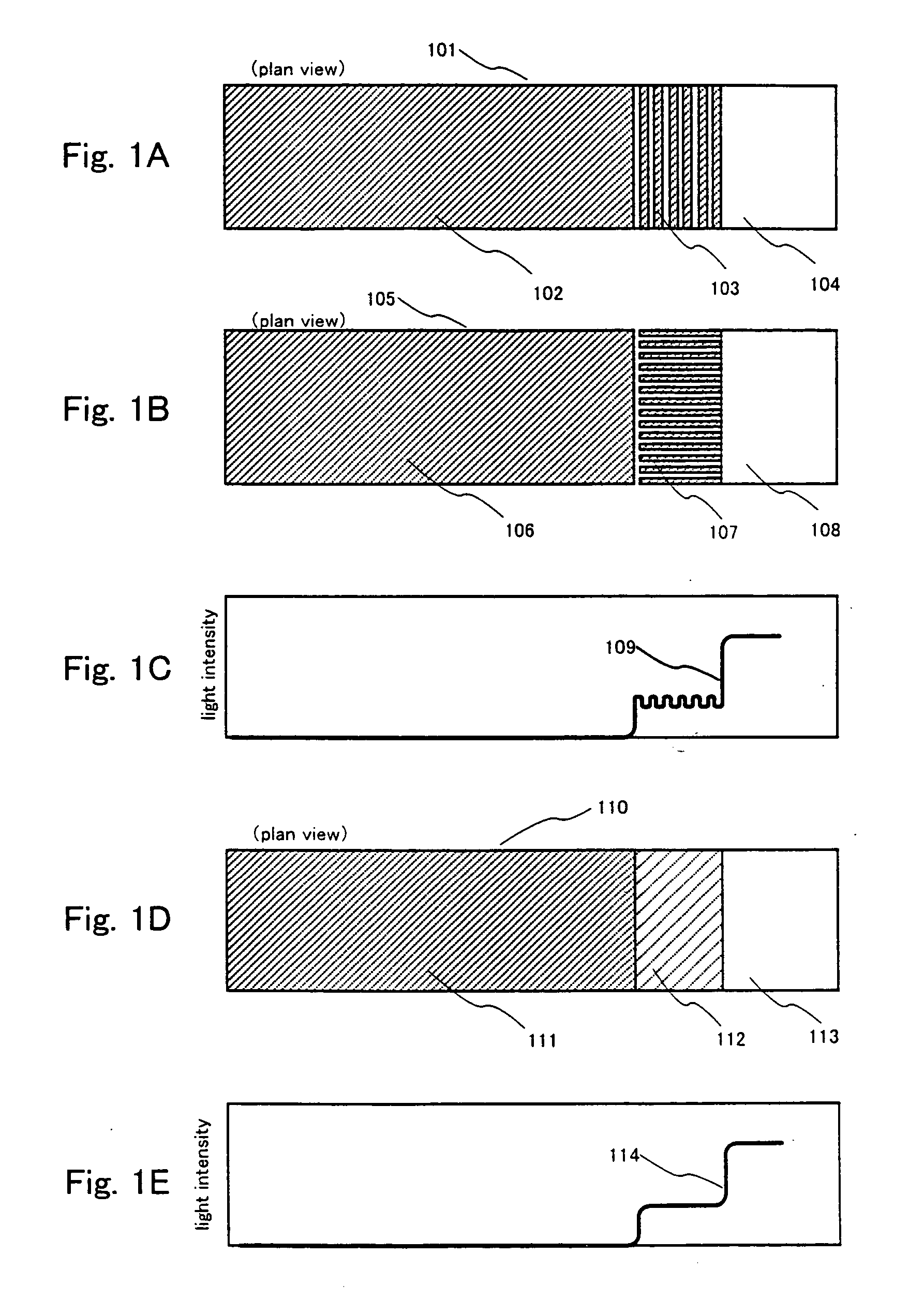
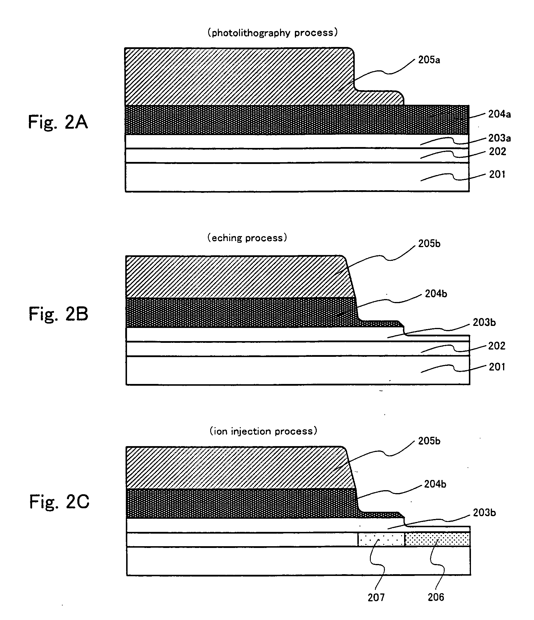
[0091] A case of applying a photolithography process that utilizes a photomask, or a reticle, for forming a gate electrode having a function of reducing the intensity of light and which is made from a diffraction grating pattern or a translucent film, for forming GOLD structure polycrystalline silicon TFT, is stated based on FIGS. 1A to 1E and FIGS. 2A to 2C.
[0092] First, a structure of a photomask, or a reticle, used for forming a gate electrode and in which is set a supplemental pattern made from a diffraction grating pattern, or a translucent film, and which has a function of reducing the intensity of light, is explained using FIGS. 1A to 1E.
[0093] A supplemental pattern having a function of reducing the intensity of light is established in edge portions of one side, or both sides, of a mask pattern in a photomask, or a reticle, used for forming a gate electrode. Examples of a diffraction grating pattern having a slit portion composed of lines and spaces below the limit of reso...
embodiment mode 2
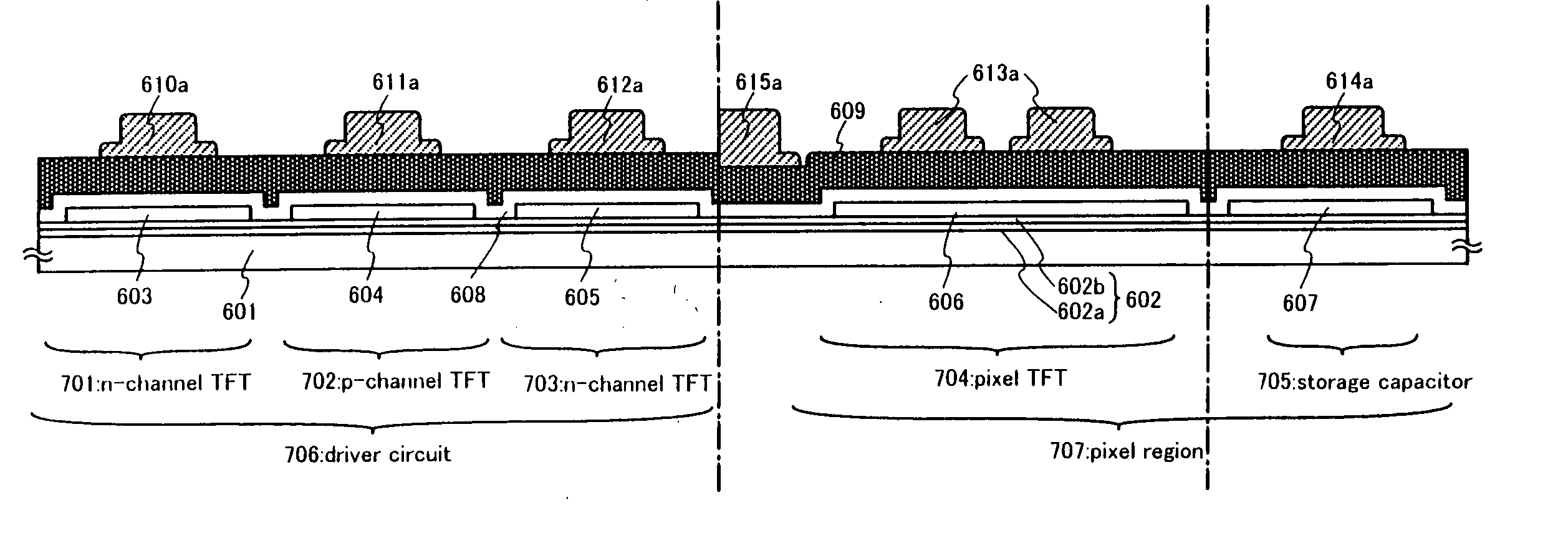
[0103] Various types of circuits are included in a semiconductor device such as a liquid crystal display, and although there are cases in which a GOLD structure having a superior effect against hot carriers is suitable, there are also cases in which an LDD structure having a small off current value are appropriate. Single drain structures may also be suitable, depending upon the circumstances. It is therefore necessary to form GOLD structure, LDD structure, and single drain structure polycrystalline silicon TFTs separately for each circuit. In embodiment mode 2, a method of forming GOLD structure, LDD structure, and single drain structure polycrystalline silicon TFTs separately for each circuit is discussed based upon FIGS. 3A to 3D. Note that the photomasks or reticles 101, 105, and 110 used for forming the gate electrodes (see FIGS. 1A, 1B, and 1D) have already been discussed in embodiment mode 1, and therefore an explanation will be omitted here.
[0104] Concerning the substrate s...
embodiment mode 3
[0116] A case in which a photolithography process, utilizing a photomask or a reticle used for forming a gate electrode having a function of reducing the intensity of light and composed of a diffraction grating pattern or a translucent film, is applied to the formation of a GOLD structure polycrystalline silicon TFT, is discussed based on FIGS. 9A to 9E and 10A to 10C. First, a structure of a photomask, or a reticle, used for forming a gate electrode and in which a supplemental pattern made from a diffraction grating pattern, or a translucent film is set, and which has a function of reducing the intensity of light, is explained using FIGS. 9A to 9E.
[0117] A supplemental pattern having a function of reducing the intensity of light is established in edge portions of one side, or both sides, of a mask pattern in a photomask, or a reticle, used for forming a gate electrode such that transmittivity is gradually increased in proportion to distance from mask pattern. Examples of a diffrac...
PUM
| Property | Measurement | Unit |
|---|---|---|
| temperature | aaaaa | aaaaa |
| channel length | aaaaa | aaaaa |
| pressure | aaaaa | aaaaa |
Abstract
Description
Claims
Application Information