Porous substrate and its manufacturing method, and gan semiconductor multilayer substrate and its manufacturing method

a technology of porous substrates and manufacturing methods, applied in the direction of polycrystalline material growth, chemically reactive gases, crystal growth processes, etc., can solve the problems of defect becoming an obstacle, the lattice mismatch between the substrate and the crystal cannot be eliminated, and the single crystal film cannot be grown by directly growing gan on the sapphire substra

Inactive Publication Date: 2006-03-02
SUMITOMO CHEM CO LTD
View PDF4 Cites 42 Cited by
  • Summary
  • Abstract
  • Description
  • Claims
  • Application Information

AI Technical Summary

Benefits of technology

[0022] (8) A fabrication method for a GaN series semiconductor layered substrate of the present invention is characterized by including growing two or more different material layers on the

Problems solved by technology

Since the sapphire substrate has a different lattice constant from GaN, a single-crystal film cannot be grown by directly growing GaN on the sapphire substrate.
However, the lattice mismatch between the substrate and the crystal cannot be obviated even by this method, and GaN obtained has a dislocation of 1019-1010 cm−2.
This defect becomes an obstacle in fabricating a GaN series LD.
This process comprises a SiO2 film depositing step by CVD or the like, a resist coating step, a photolithography step, an etching and cleaning step, etc.,

Method used


Image

  • Porous substrate and its manufacturing method, and gan semiconductor multilayer substrate and its manufacturing method
  • Porous substrate and its manufacturing method, and gan semiconductor multilayer substrate and its manufacturing method
  • Porous substrate and its manufacturing method, and gan semiconductor multilayer substrate and its manufacturing method

Examples


embodiment 1

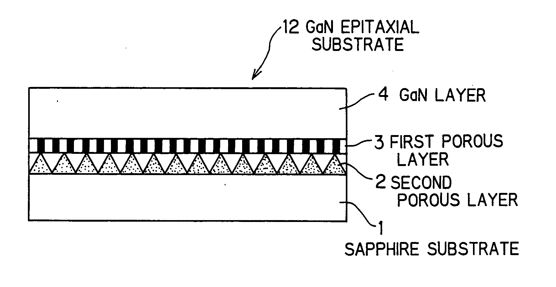
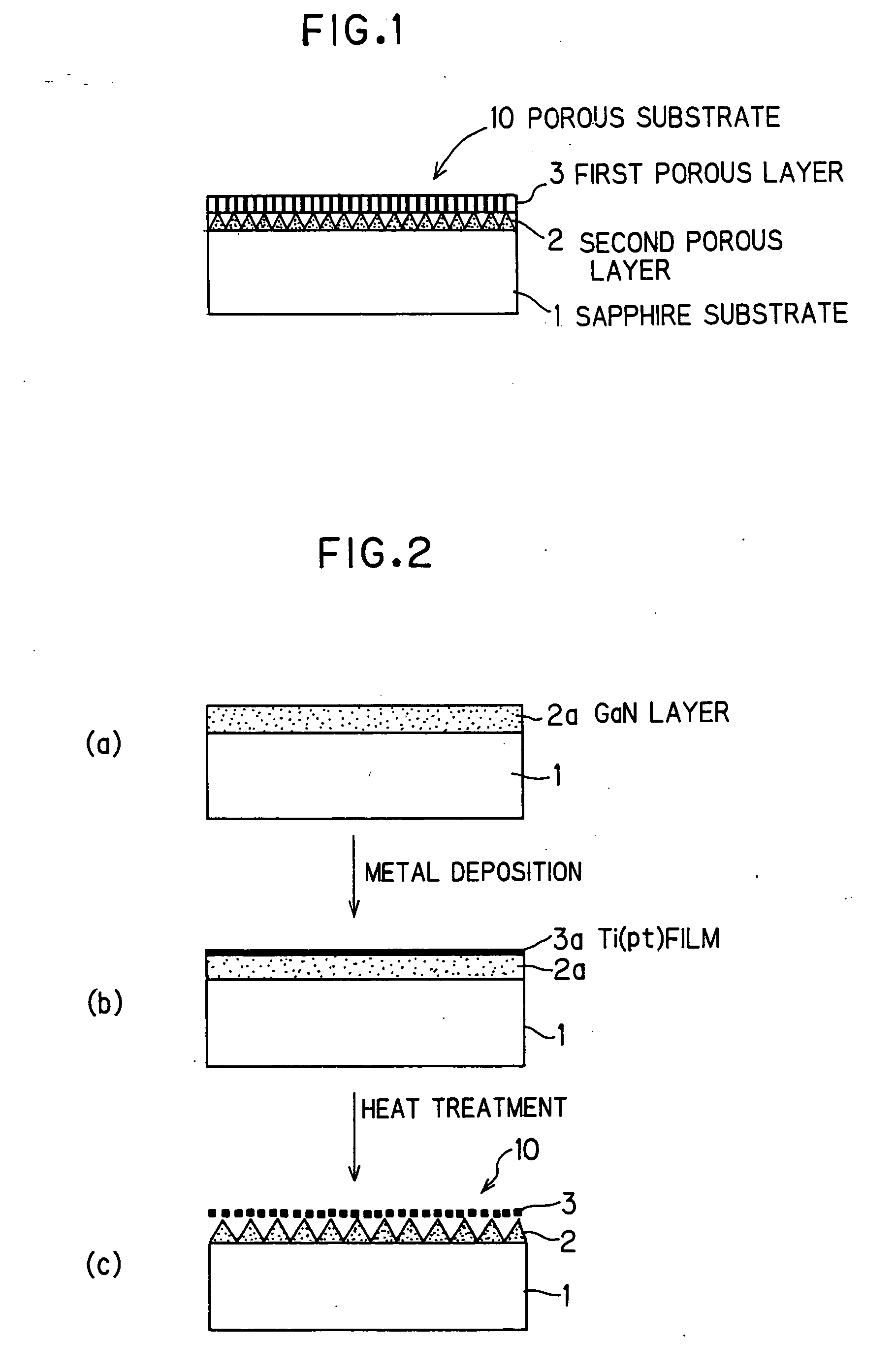
[0052]FIG. 1 illustrates a porous substrate 10 where a second porous layer 2 comprising GaN is formed on a single-crystal sapphire substrate 1, and a first porous layer 3 comprising a metal nitride such as TiN or the like is formed on the second porous layer 2.

[0053] The process for fabricating the porous substrate 10 illustrated in FIG. 1 will be explained.

[0054] As shown in FIG. 2 (a), a GaN layer 2a was grown 500 nm on a single-crystal sapphire C-face substrate 1 with a diameter of 2 inches, with MOVPE, using TMG and NH3.

[0055] Subsequently, a metal Ti film 3a was deposited 20 nm on the GaN layer 2a using a vacuum deposition apparatus (FIG. 2 (b)) This was inserted into an electric furnace, and was heated in a H2 gas stream mixed with NH3 20%, at 1040° C. for 20 min.

[0056] As a result, as shown in FIG. 2 (c), part of the GaN layer 2a was etched to cause the occurrence of high-density pores so that a second porous layer 2 was formed, while at the same time the Ti film 3a was n...

embodiment 2

[0060]FIG. 5 shows an example where a GaN crystal is grown on a porous substrate 10 shown in embodiment 1, with MOVPE.

[0061] The porous substrate 10 fabricated with the method of embodiment 1 was inserted into an MOCVD furnace, and was heated in an ammonia stream mixed with H2 20%, at 1050° C., for 30 min. Subsequently, in the same furnace, a GaN film 4 was grown 2 μm on the TiN layer (the first porous layer 3) at 1050° C., using TMG and NH3. Nomarski microscope and SEM observations verified that the surface of a GaN epitaxial substrate 12 obtained was very flat and in a good surface state with less microscopic irregularity in its surface, compared to an existing GaN epitaxial substrate grown on a sapphire substrate via a low-temperature growth buffer layer.

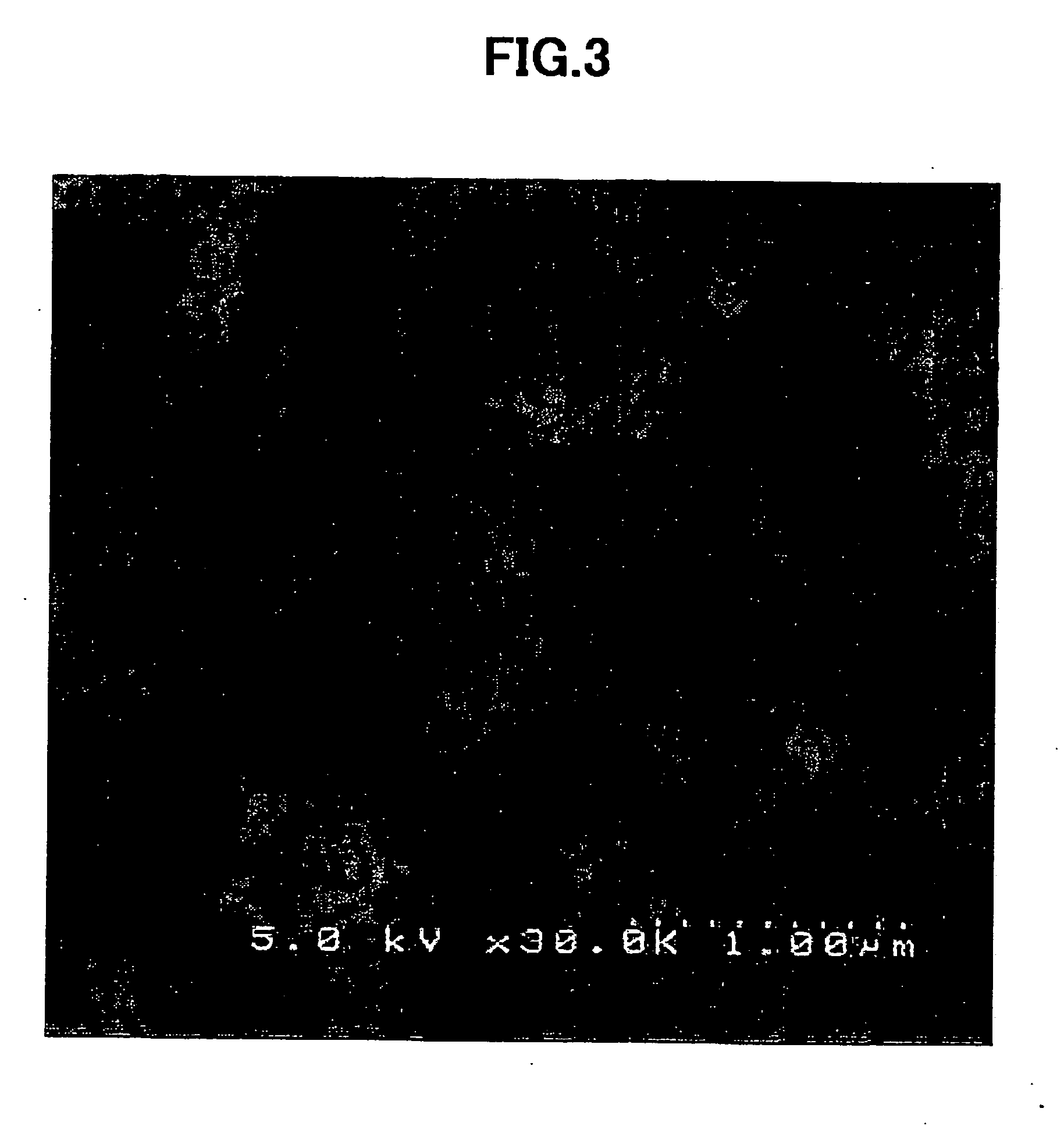
[0062] AFM (atomic force microscope) observation verified that the GaN single-crystal substrate 12 obtained had high crystalline quality, by showing that the measured density of pits (corresponding to dislocations) observed in ...

embodiment 3

[0064] An example of using Pt as first porous layer 3 material and GaN as second porous layer 2 material will be explained, referring to FIG. 2 as in Embodiment 1.

[0065] A substrate 8 was prepared having GaN layer 2a grown 0.5 μm a single-crystal sapphire C-face substrate 1 with a diameter of 2 inches, with MOVPE, using TMG and NH3. A metal Pt film 3a was deposited 20 nm on the GaN layer 2a, and this was inserted into an electric furnace, and was heated in an atmosphere, at 850° C., for 20 min. As a result, a second porous layer 2 with high-density pores analogous to FIG. 4 was formed in the GaN layer 2a, while a first porous layer 3 with high-density holes of submicrons was formed in the Pt film 3a.


PUM

PropertyMeasurementUnit
Fractionaaaaaaaaaa
Thicknessaaaaaaaaaa
Diameteraaaaaaaaaa

Abstract

A structure of a substrate used for growing a crystal layer of a semiconductor, particularly a group-III nitride semiconductor and its manufacturing method. The substrate comprises two porous layers on a base. The mean opening diameter of the pores of the first porous laser, the outermost layer, is smaller than the means diameter of the pores in the second porous layer nearer to the base than the first porous layer. The first and second porous layers have volume porosities of 10 to 90%. More then 50% of the pores of the first porous layer extend from the surface of the first porous layer and reach the interface between the first and second porous layers. Even by a conventional crystal growing method, an epitaxial crystal of low defect density can be easily grown on the porous substrate.

Description

TECHNICAL FIELD [0001] The present invention relates to a structure of a substrate used for growing a semiconductor crystal layer or the like, especially, a group III nitride semiconductor crystal layer, and a fabrication method therefor. BACKGROUND ART [0002] GaN series compound semiconductors such as gallium nitride (GaN), aluminum nitride (AlN), indium nitride (InN), indium gallium nitride (InGaN) and gallium aluminum nitride (GaAlN) have been in the limelight as materials for blue light-emitting diodes (LEDs) and laser diodes (LDs). Further, GaN series compound semiconductors begin to be applied and developed to elements for electronic devices by utilizing the characteristics of good heat- and environment-resistance. [0003] GaN series compound semiconductors have difficulty in bulk crystal growth, and therefore a GaN self-standing substrate which can withstand practical use is still developing. A substrate for GaN growth which has currently been widely put into practical use is ...

Claims


Application Information

Patent Timeline
IPC IPC(8): H01L21/31H01L21/469C30B29/38C23C16/34C30B25/02C30B25/18H01L21/205
CPCC30B25/02C30B25/18C30B29/403C30B29/406H01L21/0242H01L21/0262H01L21/02458H01L21/02491H01L21/02502H01L21/02513H01L21/0254H01L21/02439C30B29/38
Inventor SHIBATA, MASATOMOOSHIMA, YUICHIERI, TAKESHIUSUI, AKIRASUNAGAWA, HARUO
Owner SUMITOMO CHEM CO LTD
Why Eureka
Try Eureka