Semiconductor optical amplifier device amplifying an externally applied light signal, semiconductor optical amplification driving device and semiconductor light receiving apparatus

Inactive Publication Date: 2006-03-09
SHARP KK
View PDF5 Cites 7 Cited by
  • Summary
  • Abstract
  • Description
  • Claims
  • Application Information

AI Technical Summary

Benefits of technology

[0032] An object of the invention is to provide a semiconductor optical amplifier device, a semiconductor optical amplification driving device and a semiconductor optical receiv

Problems solved by technology

The increase in transmission loss leads to restriction on the allowed transmission distance.
In addition to factors inside the optical fiber, various factors deteriorate the light signal when it passes through many devices such as repeaters and switches.
Deterioration of the light signal becomes a major cause of increasing Bit Error Rate (BER).
However, the thick depletion layer of the photodiode deteriorates a high response property, and it is difficult to use such photodiodes in superfast optical communication of a large-capacity in the future.
In a conventional photodiode, holes and electrons form traveling carriers, and holes at a low traveling speed impede fast response.
Therefore, the UTC-PD is not suitable for light signals which are deteriorated due to transmission loss.
However, the method of amplifyi

Method used


Image

  • Semiconductor optical amplifier device amplifying an externally applied light signal, semiconductor optical amplification driving device and semiconductor light receiving apparatus
  • Semiconductor optical amplifier device amplifying an externally applied light signal, semiconductor optical amplification driving device and semiconductor light receiving apparatus
  • Semiconductor optical amplifier device amplifying an externally applied light signal, semiconductor optical amplification driving device and semiconductor light receiving apparatus

Examples


Example

First Embodiment

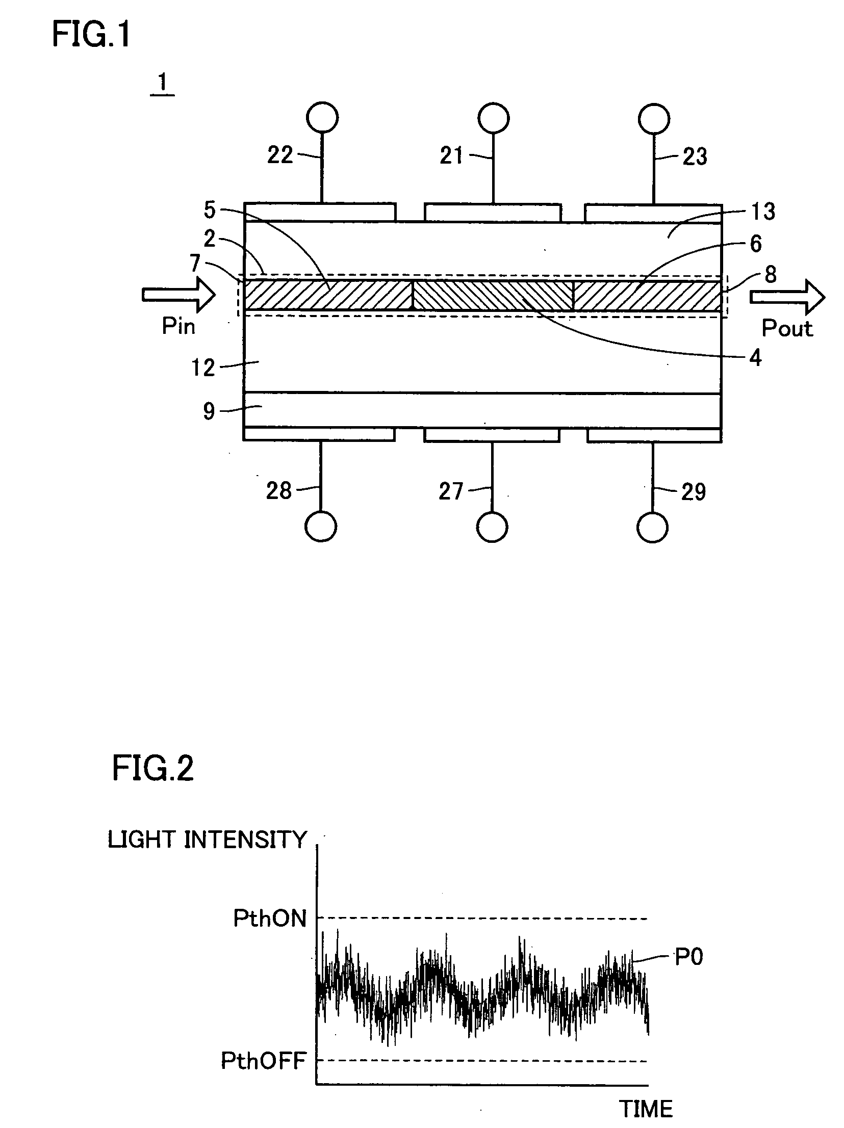
[0092]FIG. 1 is a cross section showing a schematic structure, on a side surface of an oscillator, of a semiconductor optical amplifier device 1 of a first embodiment of the invention.

[0093] Referring to FIG. 1, a semiconductor optical amplifier device 1 of a first embodiment includes an active layer 2, an n-type InP (indium phosphide) substrate 9, an n-type InP clad layer 12, a p-type InP clad layer 13, p-electrodes 21-23 and n-electrodes 27-29. n-type InP clad layer 12 is formed on n-type InP substrate 9. Active layer 2 is formed on n-type InP clad layer 12.

[0094] Active layer 2 is made of InGaAsP (Indium Gallium Arsenic Phosphide), and includes a saturable absorption region 4 and optical amplification regions 5 and 6. On a side surface of an oscillator in semiconductor optical amplifier device 1, optical amplification regions 5 and 6 are located on the opposite sides of saturable absorption region 4, respectively. Optical amplification region 5 has an incidence...

Example

Second Embodiment

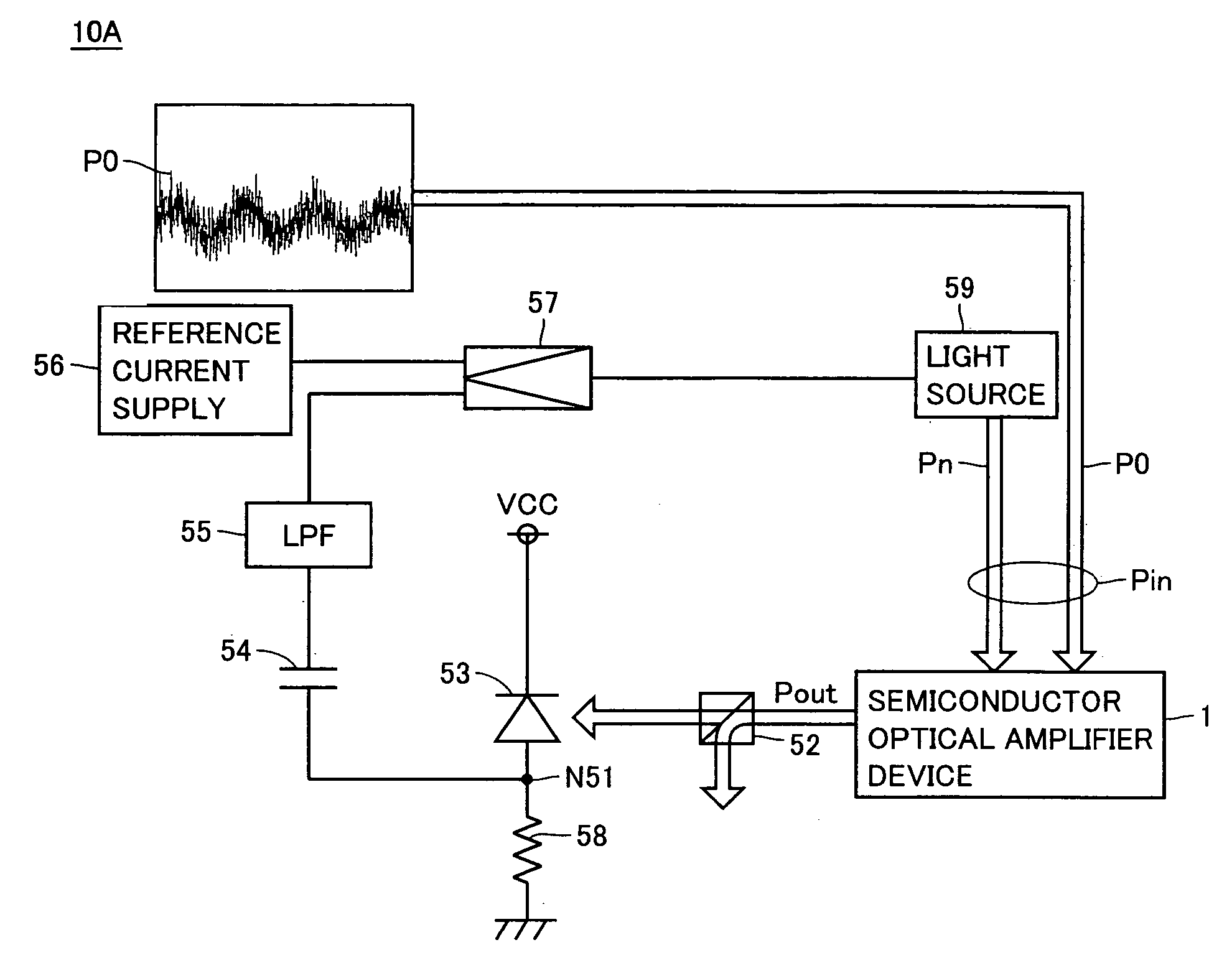
[0153]FIG. 7 shows a schematic structure of a semiconductor optical amplification driving device 10A of a second embodiment of the invention.

[0154] Referring to FIG. 7, semiconductor optical amplification driving device 10A of the second embodiment is formed of semiconductor optical amplifier device 1 and its driving device. More specifically, semiconductor optical amplification driving device 10A includes semiconductor optical amplifier device 1, a beam splitter 52, a photoelectric converter 53, a coupling capacitor 54, a low-pass filter (LPF) 55, a reference current supply 56, a preamplifier 57, a resistance 58 and a light source 59.

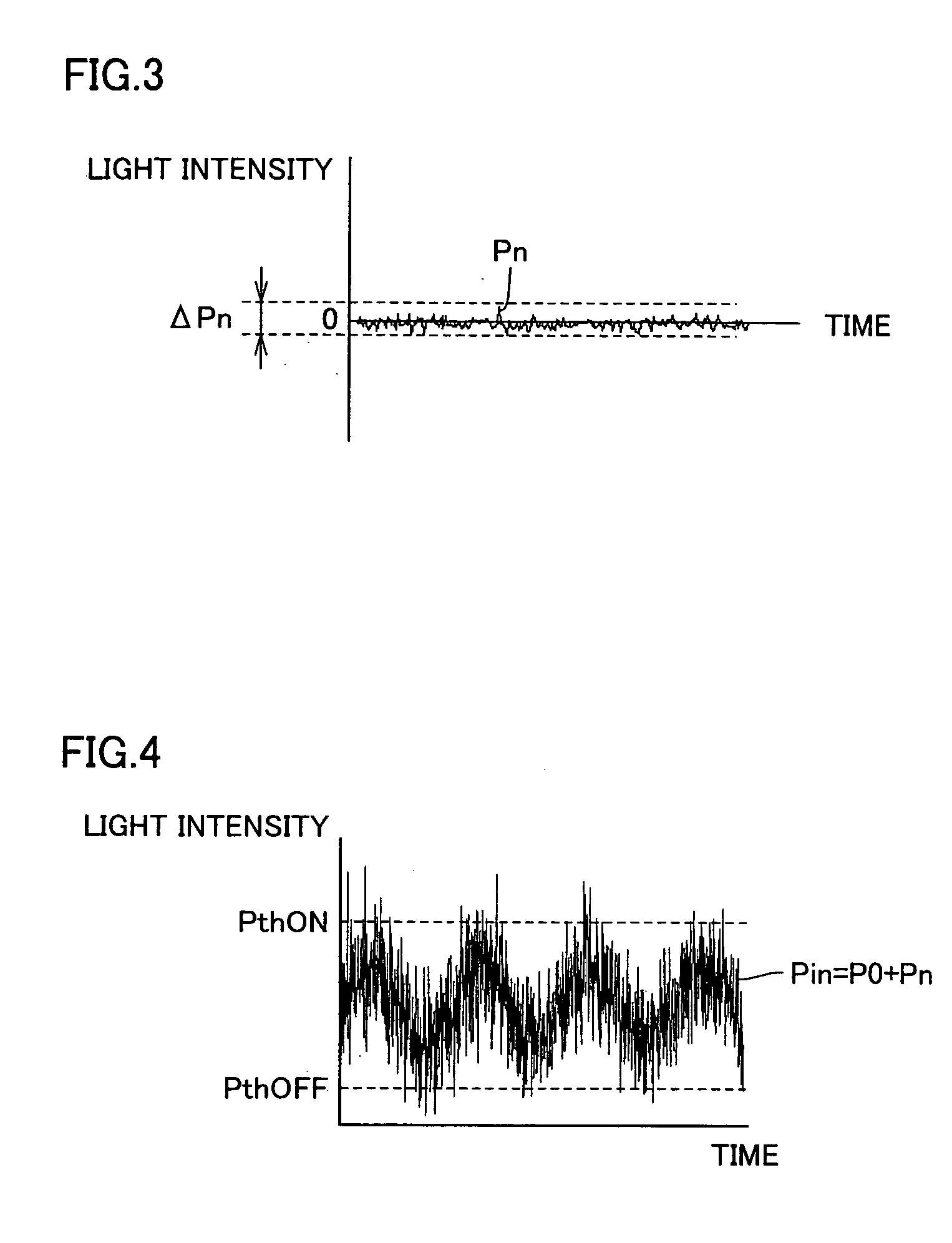
[0155] Semiconductor optical amplifier device 1 shown in FIG. 7 is the same as the semiconductor optical amplifier devices in the bistable state which have the saturable absorption regions, and are already described in connection with the first embodiment and its first to fourth modifications. Therefore, description of the same or c...

Example

Third Embodiment

[0165]FIG. 8 shows a schematic structure of a semiconductor optical amplification driving device 10B of a third embodiment of the invention.

[0166] Referring to FIG. 8, semiconductor optical amplification driving device 10B of the third embodiment is formed of semiconductor optical amplifier device 1 and its driving device. More specifically, semiconductor optical amplification driving device 10B includes semiconductor optical amplifier device 1, modulated current supply circuits 68 and 69, a beam splitter 77, a photoelectric converter 78 and a feedback control circuit 79.

[0167] Semiconductor optical amplifier device 1 shown in FIG. 8 is the same as the semiconductor optical amplifier devices in the bistable state which have the saturable absorption regions, and are already described in connection with the first embodiment and its first to fourth modifications. Therefore, description of the same or corresponding portions is not repeated. Operation characteristics o...


PUM


Abstract

A semiconductor optical amplifier device includes an active layer, an n-type InP substrate, an n-type InP clad layer, a p-type InP clad layer, p-electrodes and n-electrodes. The active layer is made of, e.g., InGaAsP, and includes a saturable absorption region and optical amplification regions. A common modulated current is injected into each optical amplification region through the p-electrode. A modulated current is injected into the saturable absorption region through the p-electrode independently of the optical amplification region. The active layer receives injection light produced by adding additional noise light to an externally applied light signal, and emits output light produced by amplifying the injection light.

Description

[0001] This nonprovisional application is based on Japanese Patent Application No. 2004-257062 filed with the Japan Patent Office on Sep. 3, 2004, the entire contents of which are hereby incorporated by reference. BACKGROUND OF THE INVENTION [0002] 1. Field of the Invention [0003] The present invention relates to a semiconductor optical amplifier device, a semiconductor optical amplification driving device and a semiconductor light receiving apparatus, and particularly to a semiconductor optical amplifier device amplifying an externally applied light signal as well as a semiconductor optical amplification driving device and a semiconductor light receiving apparatus. [0004] 2. Description of the Background Art [0005] At present, optical communication systems transmit light signals having modulated intensities through optical fibers. The light signal is reflected by an inner wall of the fiber many times when it moves through the fiber, and the signal intensity decreases due to absorpt...

Claims


Application Information

Patent Timeline
IPC IPC(8): H03F3/08
CPCH01L31/101H01S5/0601H03F3/08H01S5/5027H01S5/50
Inventor MATSUDA, KYOKOOKUMURA, TOSHIYUKI
Owner SHARP KK
Why Eureka
Try Eureka