Silicon carbide semiconductor device and its method of manufacturing method

Inactive Publication Date: 2006-03-16
SANYO ELECTRIC CO LTD SHARE 20 +1
View PDF8 Cites 62 Cited by
  • Summary
  • Abstract
  • Description
  • Claims
  • Application Information

AI Technical Summary

Benefits of technology

[0053] A second region provided in a low concentration p-type deposition film is wider than the first region provided in the high concentration p+ deposition film, reducing the resistance components from that portion, thereby lowering the ON-resistance. When the gate insulation film over the n-type base region is made thicker than the low concentration gate region and a positive gate voltage is applied, there is a decrease in the number of conduction electrons in th

Problems solved by technology

Also, the implanted p-type impurity elements are not adequately electrically activated even by applying heat treatment at high temperatures above 1600° C. Therefore, in order to obtain a sufficient impurity concentration, it is necessary to increase the injection amount, which increases the amount of defects that are produced.
As a result, the conduction electrons in the channel are scattered by these defects and the like, reducing mobility.
Thus, a problem with silicon carbide planar type vertical MOSFETs manufactured by the double ion implantation method is that channel mobility is 1 cm2/Vs or lower, which is very low, and the ON-resistance is far higher than the theoretical level.
Doing that means that the acceleration voltage for the implantation of n-type impurity ions for forming the low concentration n-type base region 4 becomes very high, in the MeV range, making it difficult to manufacture an apparatus using an ordinary apparatus.
However, increasing the blocki

Method used


Image

  • Silicon carbide semiconductor device and its method of manufacturing method
  • Silicon carbide semiconductor device and its method of manufacturing method
  • Silicon carbide semiconductor device and its method of manufacturing method

Examples


first embodiment

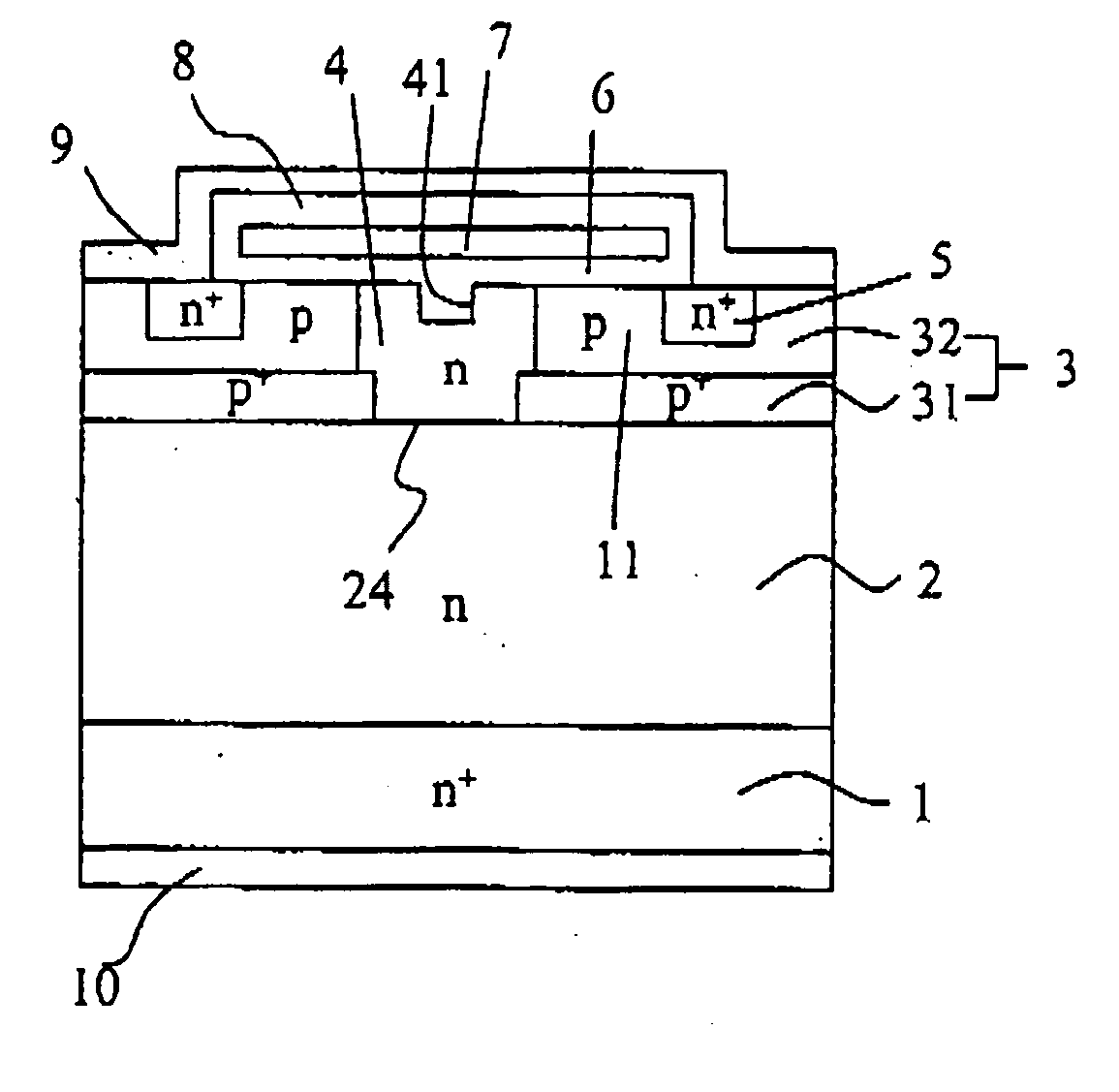
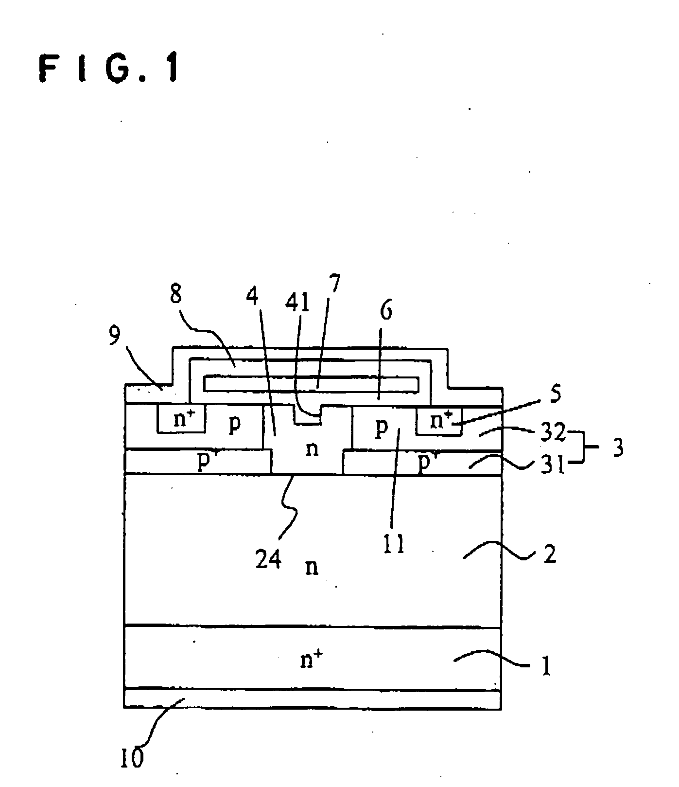
[0073]FIG. 1 is a schematic cross-sectional drawing for explaining a unit cell of a silicon carbide vertical MOSFET according to the invention. In FIG. 1, a low concentration n-type drift layer 2 having a thickness of 10 μm and a nitrogen doping concentration of 5×1015 cm−3, for example, is deposited on the surface of a high concentration n+ substrate 1 having a (0001) surface, a thickness of 300 μm and a nitrogen doping concentration of 1×1018 cm−3, for example.

[0074] A high concentration p+ layer 31 having a thickness of 0.5 μm and an aluminum doping concentration of 2×1018 cm−3, for example, is formed on the low concentration n-type drift layer 2. Then, a low concentration p-type layer 32 having a thickness of 0.5 μm and an aluminum doping concentration of 5×1015 cm−3, for example, is formed on the high concentration p+ layer 31. A high concentration n+ source region 5 that is selectively doped with about a 1×1020 cm−3 concentration of phosphorus is formed in a surface portion of...

second embodiment

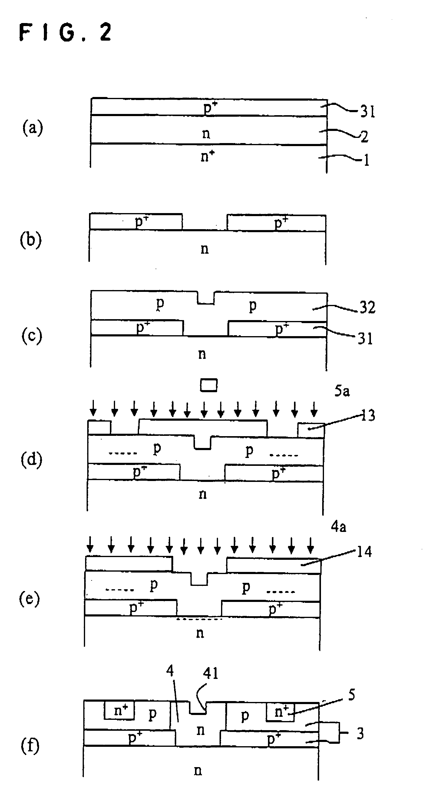
[0087]FIG. 4 is a schematic cross-sectional drawing for explaining the unit cell of a silicon carbide vertical MOSFET according to the invention. With reference to FIG. 4, a low concentration n-type drift layer 2 having a thickness of 10 μm and a nitrogen doping concentration of 5×1010 cm−3 is deposited on the (0001) surface of a 300 μm-thick high concentration n+ substrate 1 having a nitrogen doping concentration of 5×1018 cm−3. Aluminum doping at a concentration of 2×1018 cm−3 is used to form a high concentration p+ layer 31 extending down to a depth of 0.5 μm from the surface of the low concentration n-type drift layer 2, and a 0.5-μm-thick low concentration p-type layer 32 having an aluminum doping concentration of 5×1015 cm−3 is deposited on the surface of the layer 31.

[0088] A high concentration n+ source region 5 that is selectively doped with phosphorus at a concentration of approximately 1×1020 cm−3 is formed in the surface portion of the low concentration p-type layer 32. ...


PUM


Abstract

A silicon carbide vertical MOSFET having low ON-resistance and high blocking voltage. A first deposition film of low concentration silicon carbide of a first conductivity type is formed on the surface of a high concentration silicon carbide substrate of a first conductivity type. Formed on the first deposition film is a second deposition film that includes a high concentration gate region of a second conductivity type, with a first region removed selectively. A third deposition film is formed on the second deposition film, which includes a second region that is wider than the selectively removed first region, a high concentration source region of a first conductivity type, and a low concentration gate region of a second conductivity type. A low concentration base region of a first conductivity type is formed in contact with the first deposition film in the first and second regions.

Description

TECHNICAL FIELD [0001] The present invention relates to a vertical MOSFET device manufactured on a silicon carbide substrate, and to a method of manufacturing same. BACKGROUND ART [0002] Compared with silicon (Si), silicon carbide (SiC) has a number of superior properties, such as 1. a wider bandgap, 2. a higher dielectric breakdown strength and 3. a higher electron saturation drift velocity. As such, using silicon carbide as a substrate material makes it possible to manufacture low-resistance power semiconductor devices having much higher blocking voltages than silicon has. Also, as in the case of silicon, thermal oxidation can be used to form an insulation layer on silicon carbide. For this reason, considerable research and development is being conducted into producing vertical MOSFETs having a low ON-resistance and high blocking voltages, using silicon carbide as the substrate material. [0003]FIG. 12 is a schematic cross-sectional view for explaining a unit cell of a typical plan...

Claims


Application Information

Patent Timeline
IPC IPC(8): H01L21/8238H01L21/04H01L29/10H01L29/24H01L29/423H01L29/78
CPCH01L21/0465H01L29/1095H01L29/1608H01L29/66477H01L29/66068H01L29/7802H01L21/02529H01L29/42368
Inventor HARADA, SHINSUKEYATSUO, TSUTOMUFUKUDA, KENJIOKAMOTO, MITSUOADACHI, KAZUHIRO
Owner SANYO ELECTRIC CO LTD SHARE 20
Why Eureka
Try Eureka