

Ink composition for etching resist, method of forming etching resist pattern using the same, and method of forming microchannel using the ink composition
- Summary
- Abstract
- Description
- Claims
- Application Information
AI Technical Summary
Benefits of technology
Problems solved by technology
Method used
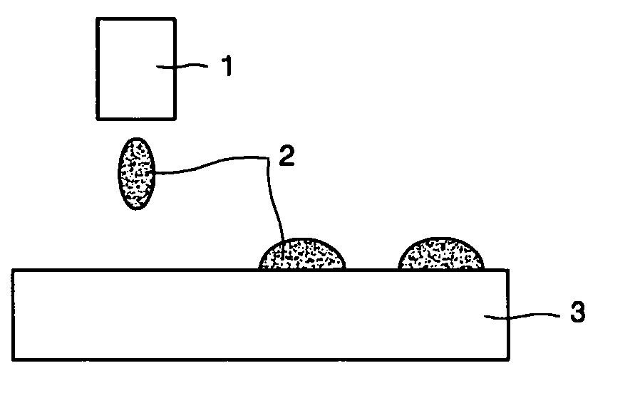
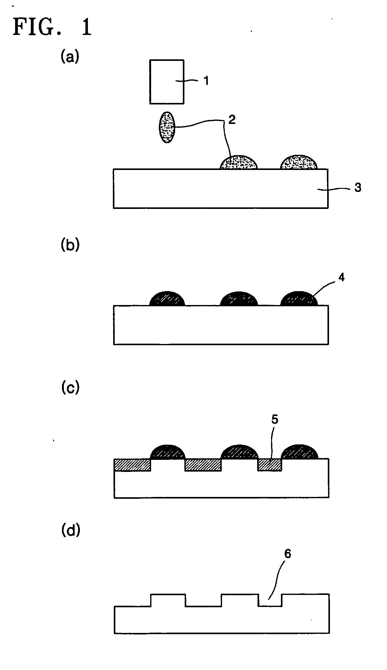
Image


Examples
example
[0066] Manufacturing Example 1
[0067] 10 parts by weight of a urethane acryl emulsion (in a dry weight), 5 parts by weight of a polytetrafluoroethylene-dispersed solution, 10 parts by weight of glycerol, 20 parts by weight of ethyleneglycol, 0.1 parts by weight of a fluorine-based surfactant, and 54.9 parts by weight of deionized water were mixed in a mixer, and then filtered using a 1-micron filter to produce an ink for an etching resist. The ink exhibited a contact angel of 35° on the surface of copper and a contact angle of 55° on the surface of stainless steel. Thus, the ink exhibited a larger contact angle and thus spread less than a conventional organic solvent.
[0068] Manufacturing Example 2
[0069] 10 parts by weight of ethoxylated glycerin acrylate, 20 parts by weight of ethyleneglycol, 0.1 parts by weight of a fluorine-based surfactant, and 69.9 parts by weight of deionized water were mixed in a mixer, and then, filtered using a 1-micron filter to prepare an ink for an etch...
example 1
[0070] A copper substrate was cleaned using 5% a hydrochloric acid aqueous solution and a deionized water, and then dried. The ink prepared in Manufacturing Example 1 was sprayed onto the cleaned copper substrate using an inkjet head produced by MICROFAB Co. USA to form a microchannel pattern. Then, the result was dried on a thermal plate at 80° C. for 3 minutes, completely cured on an oven at 220° C. for 30 minutes or longer, and then etched using an etching solution that contained 17 parts by weight of iron chloride and 20 parts by weight of hydrochloric acid for 30 minutes. Subsequently, the remaining etching resist pattern was removed by brushing the etched result in acetone, so that portions of the copper substrate that were not covered by the etching resist pattern were etched to a depth of 50 microns or greater and a width of 50 microns or less. As a result, a microchannel pattern was formed.
example 2
[0071] A stainless steel substrate was rubbed with a nonwoven fabric to which a polishing agent was attached, cleaned with a 10% aqueous sulfuric acid solution, 6% (1-hydroxyethylene)diphosphonic acid (obtained from Sigma Aldrich USA), and deionized water, and then dried. The ink prepared in Manufacturing Example 2 was sprayed onto the resulting substrate using an inkjet head produced by MICROFAB USA to form a microchannel pattern. Then, the result was dried on a thermal plate at 300° C. for 30 minutes or greater, and then etched using an etching solution that contains contained 17 parts by weight of iron chloride and 20 parts by weight of hydrochloric acid for 2 hours. Subsequently, the remaining etching resist pattern was removed by brushing the etched result in acetone, so that portions of the substrate that were not covered by the etching resist pattern were etched to a depth of about 150 microns or greater and a width of 50 microns or less. As a result, a microchannel pattern w...
PUM
| Property | Measurement | Unit |
|---|---|---|
| Percent by mass | aaaaa | aaaaa |
| Percent by mass | aaaaa | aaaaa |
| Percent by mass | aaaaa | aaaaa |
Abstract
Description
Claims
Application Information