Trimethylgallium, a method for producing the same and a gallium nitride thin film grown from the trimethylgallium

Inactive Publication Date: 2006-04-13
SUMITOMO CHEM CO LTD
View PDF11 Cites 30 Cited by
  • Summary
  • Abstract
  • Description
  • Claims
  • Application Information

AI Technical Summary

Benefits of technology

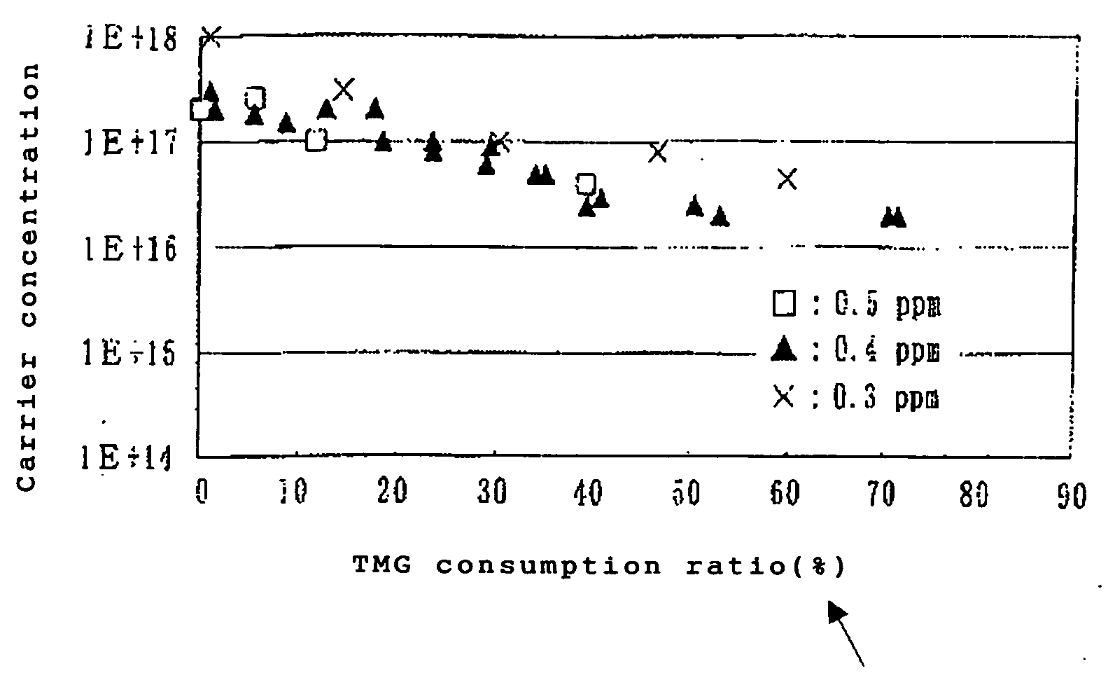
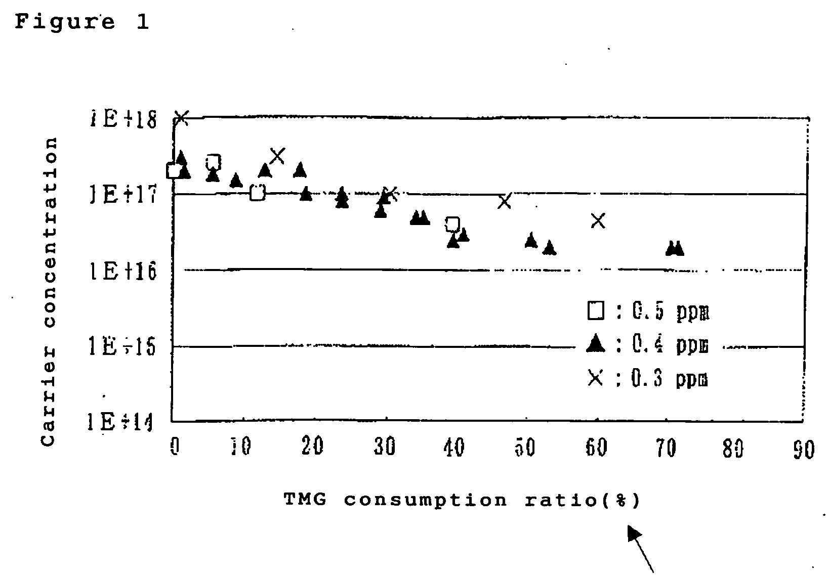
[0011] The inventors of the invention have diligently studied to stabilize carrier concentration, found the facts that organic silicon compound among the impurities affects stability of a carrier concentration, application of a trimethylgallium having less than 0.1 ppm of a total content of silicon compound allows the carrier concentration of non-doped GaN to be stably controlled being equal to or less than 1×1016 cm−3, therefore, the carrier concentration of both of n-type and p-type layers obtained by being doped with impurities can be stably adjusted in high level; and the trimethylgallium can be produced by quantifying methyltriethylsilane in trimethylaluminum as a raw material by a Gas Chromatography-Mass Spectrometry, selecting a trimethylaluminum having less than 0.5 ppm of methyltriethylsilane content for the raw material, purifying the selected trimethylaluminum by distillation, followed by reaction with gallium chloride to obtain a reactant and then distilling the reactant solution to obtain a trimethylgallium; and achieved the invention.
[0015] Conducting the content of total organic silicon compounds in the trimethylgallium less than 0.1 ppm makes it possible to stably control the carrier concentration of non-doped GaN equal to or less than 1×1016 cm−3; consequently, to stably adjust in high level the carrier concentration of both of n-type and p-type layers obtained by impurity doping.
[0021] The carrier concentration of this gallium nitride thin film is stable.

Problems solved by technology

While impurities are doped in order to adjust the carrier concentration, the carrier concentration is not necessarily dispersed uniformly in the layer.
It is well known that the quality of thin-film semiconductors deteriorated by the impurities, such as inorganic silicon contained in the organic metal compound used as a raw material.

Method used


Image

  • Trimethylgallium, a method for producing the same and a gallium nitride thin film grown from the trimethylgallium
  • Trimethylgallium, a method for producing the same and a gallium nitride thin film grown from the trimethylgallium

Examples


examples

[0052] The invention is explained by referring to Examples and Comparative Examples as follows, but should not be limited thereto.

(Analysis of Raw TMAs)

[0053] The raw TMA (1), TMA (2) and TMA (3), which were different in their supplier and grade, were analyzed about organic silicon compounds.

[0054] 11.3 g of TMA (1) was diluted with 143.6 g of xylene and mixed. Into a hydrolysis vessel filled with 80 ml of acid solution which was 36% by weight of hydrochloric acid diluted in half, the TMA solution diluted with xylene was dropped to hydrolyze the TMA where the temperature of hydrolysis solution was maintained at about −5 to −20° C. by cooling as well as adjusting the dripping amount of the TMA. The gas generated by hydrolysis was absorbed with the absorption vessel filled with 30 ml of xylene. After dropping of TMA finished, the solution was stirred for about 10 minutes to complete hydrolysis.

[0055] After hydrolysis being completed, the hydrolysis solution and the absorption sol...


PUM


Abstract

The present invention provides a trimethylgallium which has less than 0.1 ppm of a total organic silicon compound content; and a method for producing the trimethylgallium comprises hydrolyzing trimethylaluminum as a raw material, extracting organic silicon compound contained with a solvent, quantifying methyltriethylsilane by a Gas Chromatography-Mass Spectrometry, selecting a trimethylaluminum having less than 0.5 ppm of methyltriethylsilane content for the raw material, purifying by distillation, followed by reaction with gallium chloride and then distilling the reactant solution to obtain the trimethylgallium.

Description

FIELD OF THE INVENTION [0001] The present invention relates to a trimethylgallium, a method for producing the same and a gallium nitride thin film grown from the trimethylgallium. BACKGROUND OF THE INVENTION [0002] As nitride compound semiconductors having gallium nitride compound semiconductor layer, are known, for example, semiconductors having n-type and / or p-type layer, for example, represented by a formula InxGayAlzN (each of x, y and z is from 0 to 1, wherein x+y+z=1), as a layer of gallium nitride compounds grown on a sapphire substrate. The one having both of n-type and p-type layer is used as a material for a light emitting device such as a light emitting diode emitting ultra violet, blue or green colors, or laser diode emitting ultra violet, blue or green colors. [0003] Such nitride compound semiconductors are produced in a multi-layer structure including a gallium nitride thin layer by a methods such as a molecular beam epitaxy method (hereinafter abbreviated as MBE), a m...

Claims


Application Information

Patent Timeline
IPC IPC(8): C30B23/00C30B25/00C30B28/12C30B28/14C07F5/00C30B25/02C30B29/40
CPCC07F5/00C30B25/02C30B29/406C01G15/00
Inventor MATSUBARA, MASANOBUSHIMADA, KENNISHIKAWA, NAOHIROKADOTA, YOICHI
Owner SUMITOMO CHEM CO LTD
Why Eureka
Try Eureka