Laser processing unit, laser processing method, and method for manufacturing semiconductor device

Inactive Publication Date: 2006-04-13
SEMICON ENERGY LAB CO LTD
View PDF21 Cites 33 Cited by
  • Summary
  • Abstract
  • Description
  • Claims
  • Application Information

AI Technical Summary

Benefits of technology

[0028] In this invention, by blowing a gas locally at high temperature so as to overlap at a laser spot on a semiconductor film, an energy de

Problems solved by technology

The glass substrate is inferior in a heat resistanc

Method used


Image

  • Laser processing unit, laser processing method, and method for manufacturing semiconductor device
  • Laser processing unit, laser processing method, and method for manufacturing semiconductor device
  • Laser processing unit, laser processing method, and method for manufacturing semiconductor device

Examples


embodiment 1

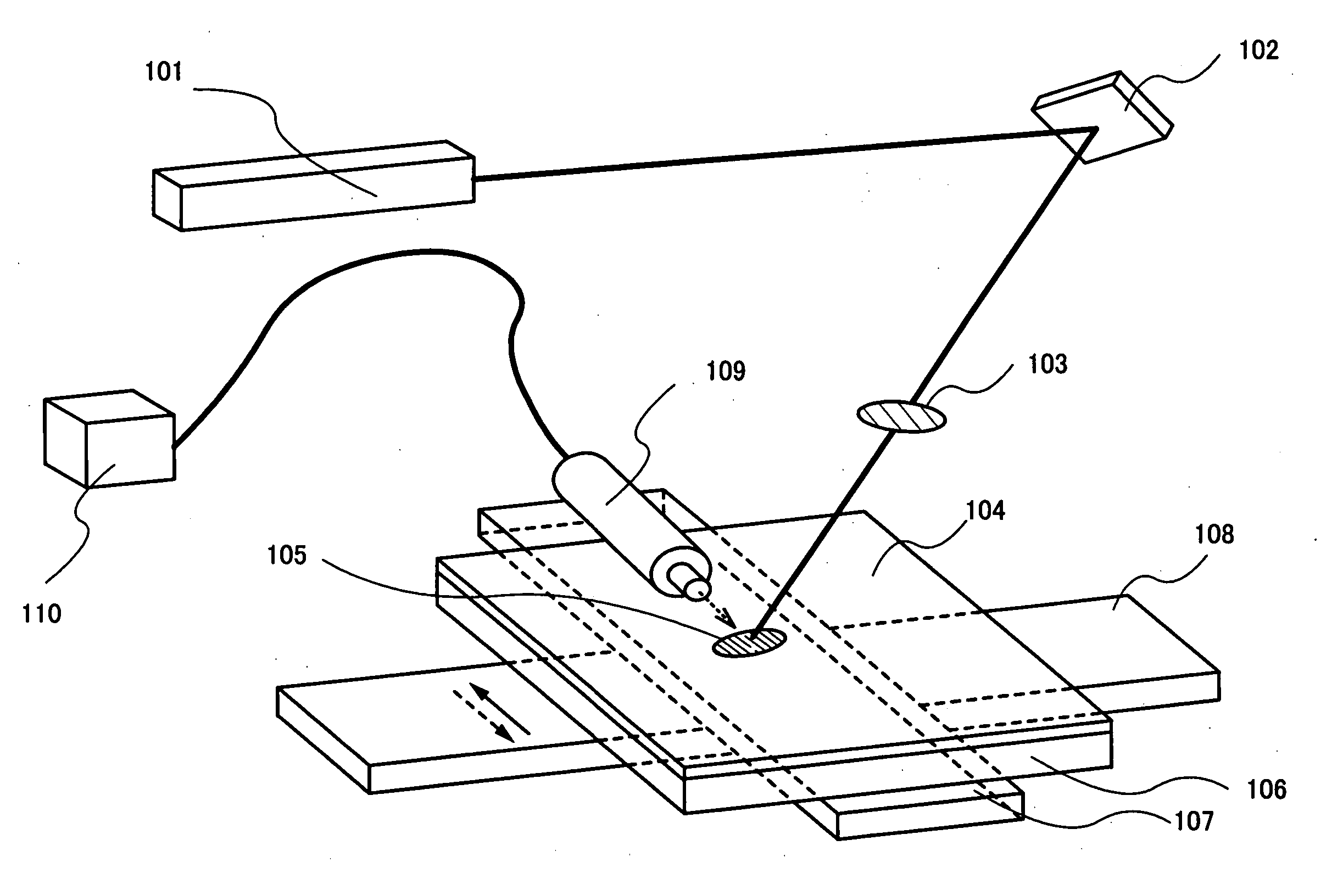
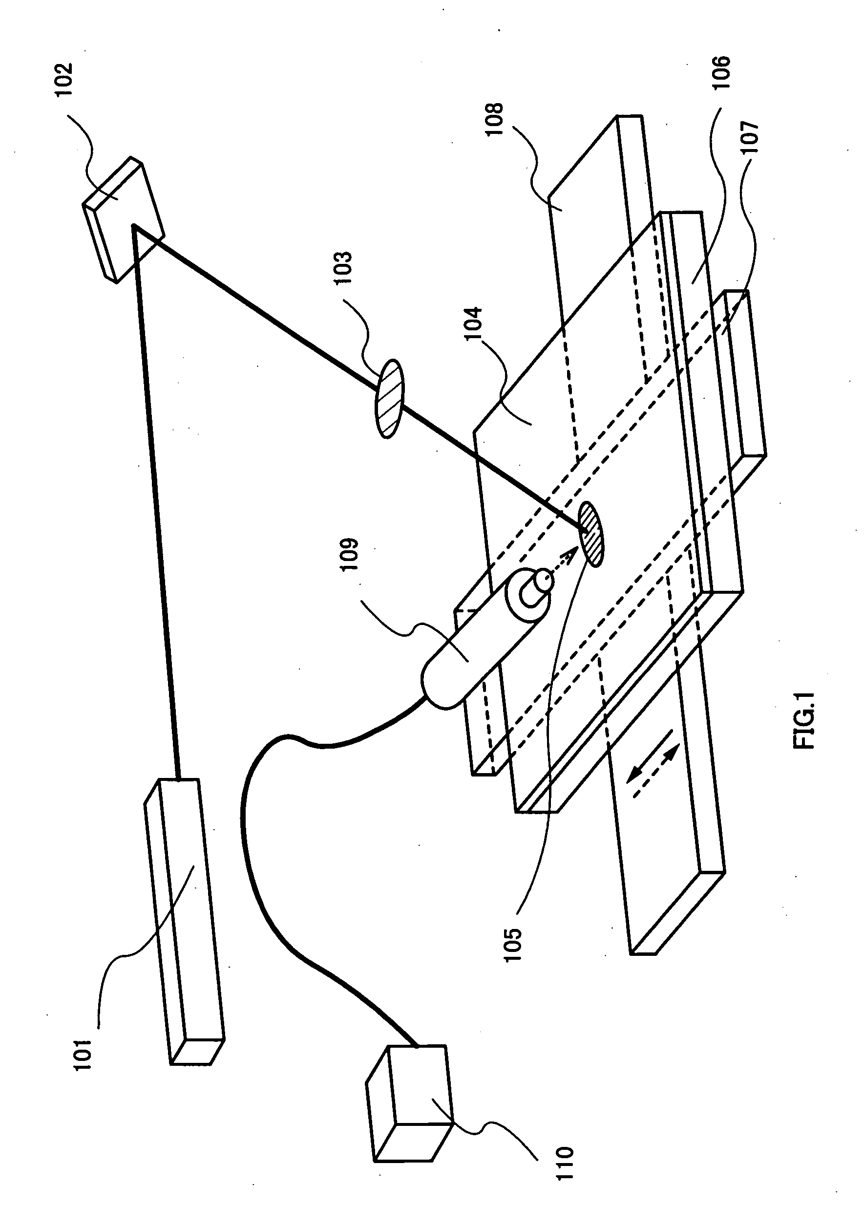
[0066] This embodiment mode is described with reference to FIG. 2, FIGS. 3(A) to 3(C), FIGS. 4(A) to 4(C), and FIGS. 5(A) to 5(C).

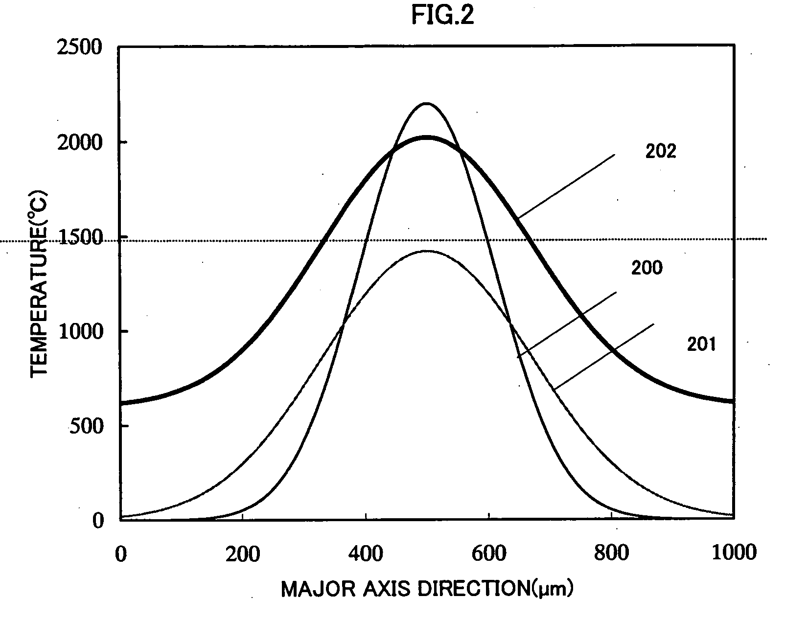
[0067] In FIG. 2, reference numeral 200 denotes temperature distribution of a linear beam in which a CW laser having a wave length of 532 nm and electric power of 10 W is formed in a linear, in a major axis direction, and the distribution generally becomes Gaussian distribution. When using an amorphous silicon film as a semiconductor film, the amorphous silicon is required to be completely melted so as to form a large grain size crystal. When the temperature for melting the amorphous silicon is supposed to be 1414° C., the length in the major axis direction of the linear beam having a temperature more than the temperature for completely melting the amorphous silicon, is approximately 200 μm. At this time, the length of a minor axis direction is to be 10 μm.

[0068] A full width at half maximum and strength in 201 is changed so that the integral value of 2...

embodiment 2

[0124] In this embodiment, an example of manufacturing a liquid crystal display device (LCD) is shown with reference to FIGS. 6, 7, 8, 9, and 18(A) and 18(B).

[0125] The method for manufacturing a display device described in this embodiment is a method for manufacturing a pixel portion including a pixel TFT and a TFT of drive circuit portion provided for the periphery thereof. However, for brief description, a CMOS circuit that is a basic unit concerning a drive circuit is shown.

[0126] First, based on Embodiment 1, the processes up to forming electrodes and wirings 540 to 544 in FIG. 5 (C) are carried out. The same symbol is used in the part corresponding with Embodiment 1.

[0127] Then, a third interlayer insulating film 610 is formed over the second interlayer insulating film 531 and the electrodes or the wirings 540 to 544. Note that the third interlayer insulating film 610 can be formed using the same material as the one used for the second interlayer insulating film 531.

[0128]...

embodiment 3

[0148] In this embodiment, an example for applying a droplet discharge method for dropping a liquid crystal is shown. In this embodiment, a large area substrate 1110 is used, and a manufacturing method by which 4 panels can be obtained from one substrate is shown in FIG. 10(A) to 10(D), FIGS. 11(A) and 11(B) and FIGS. 12(A) and 12(B).

[0149]FIG. 10(A) shows a cross sectional view in process of forming a liquid crystal layer by a dispenser (or ink jet). A liquid crystal material 1114 is discharged, sprayed, or dropped from a nozzle 1118 of a droplet discharge device 1116 so as to cover a pixel portion 1111 that is surrounded by a sealing member 1112. The droplet discharge device 1116 is moved in direction of an arrow in FIG. 10(A). Note that, the nozzle 1118 is moved here; however, a liquid crystal layer may be formed by fixing the nozzle and moving the substrate.

[0150]FIG. 10(B) shows a perspective view. The liquid crystal material 1114 is selectively discharged, sprayed, or droppe...


PUM

PropertyMeasurementUnit
Temperatureaaaaaaaaaa
Frequencyaaaaaaaaaa

Abstract

Objects of the present invention is to reduce a number of scanning a linear laser, to shorten the amount of time for laser annealing, and to reduce a manufacturing process, a manufacturing time, and manufacturing cost of a semiconductor device. In this invention, a gas at high temperature is locally blown so as to overlap at an irradiation surface of linear laser light. The linear laser light can be obtained by injecting laser light radiated from a laser oscillator into a lens. The gas at high temperature can be obtained by heating a gas which is compressed using a gas compressor, by a nozzle type heater. The heated has is sprayed so as to overlap with the irradiation surface of the linear laser light.

Description

FIELD OF THE INVENTION [0001] The present invention relates to a method for irradiating with a laser light. Furthermore, the invention relates to a method for manufacturing a semiconductor device using irradiation of the laser light. BACKGROUND ART [0002] Recently, a technique for manufacturing a semiconductor device, for example a thin film transistor (hereinafter, a TFT) over a substrate has made progress considerably, and application development to an active matrix type display device, for example, has made. Specifically, a TFT using a crystalline semiconductor film can be operated at high speed since the TFT has a higher electric field effect mobility (also referred to as mobility) as compared with a TFT using a conventional amorphous semiconductor film. Therefore, control of a pixel which has done by a drive circuit provided outside the substrate has been tried to be performed by a drive circuit formed over the same substrate as the pixel. [0003] A glass substrate is more promi...

Claims


Application Information

Patent Timeline
IPC IPC(8): H01L21/20H01L21/324H01L21/84
CPCB23K26/0736H01L27/1285H01L21/2026H01L21/268H01L27/12H01L29/78621H01L2924/01004H01L2924/01012H01L2924/01025H01L2924/01029H01L2924/01046H01L2924/01078H01L2924/01079H01L2924/04941H01L2924/15311H01L2924/16152H01L2924/19041H01L2224/16225H01L2224/48091H01L2224/48227H01L2924/01019H01L2924/01021H01L2924/01055H01L2924/01067H01L2924/01068B23K26/1405H01L2924/00014B23K26/142H01L2924/12044H01L21/0259H01L21/02683H01L21/02502H01L21/02422H01L21/02488H01L21/02505H01L21/0242H01L21/02672H01L21/0262H01L21/02686H01L21/02678H01L21/02532H01L21/0245H01L21/02691H01L2924/00H01L21/02675
Inventor TANAKA, KOICHIROYAMAMOTO, YOSHIAKI
Owner SEMICON ENERGY LAB CO LTD
Why Eureka
Try Eureka