Energy-efficient, laser-based method and system for processing target material

a laser-based method and target material technology, applied in the direction of manufacturing tools, semiconductor/solid-state device details, welding/soldering/cutting articles, etc., can solve the problems of liquid crystal repair, thermal runaway conditions and catastrophic damage, and the substrate and/or adjacent can be overheated and damaged

Inactive Publication Date: 2006-04-27
ELECTRO SCI IND INC
View PDF99 Cites 41 Cited by
  • Summary
  • Abstract
  • Description
  • Claims
  • Application Information

AI Technical Summary

Benefits of technology

[0086] In a construction of a system using the invention it can also be advantageous to operate the laser at pulse repetition rates exceeding the material processing rate and utilize a co...

Problems solved by technology

Depending upon the power of the beam, length of time of application of the beam, and other operating parameters, the silicon substrate and/or adjacent can be overheated and damaged.
Furthermore, if the substrate temperature rises during processing the absorption curve shifts will shift further into the infrared which can lead to thermal runaway conditions and catastrophic damage.
The problem of liquid crystal repair is similar to the problem of metal link ablation.
Furthermore, applicant's analysis on high density memory devices having multiple layers with specified pulsewidths in the ultrafast range, which is approached with the 100-300 ps used in the '437 patent, have not been satisfactory.
Overcoming this limitation would...

Method used


Image

  • Energy-efficient, laser-based method and system for processing target material
  • Energy-efficient, laser-based method and system for processing target material
  • Energy-efficient, laser-based method and system for processing target material

Examples


Embodiment Construction

Laser Processing System Architecture

[0102] Those skilled in the art can appreciate that the following embodiment can be applied to several applications in micromachining and laser processing with appropriate adjustments to parameters like laser power, energy density, spot size, wavelength, pulse width, polarization and repetition rate. The specific application to metal link blowing is described for illustrative purposes.

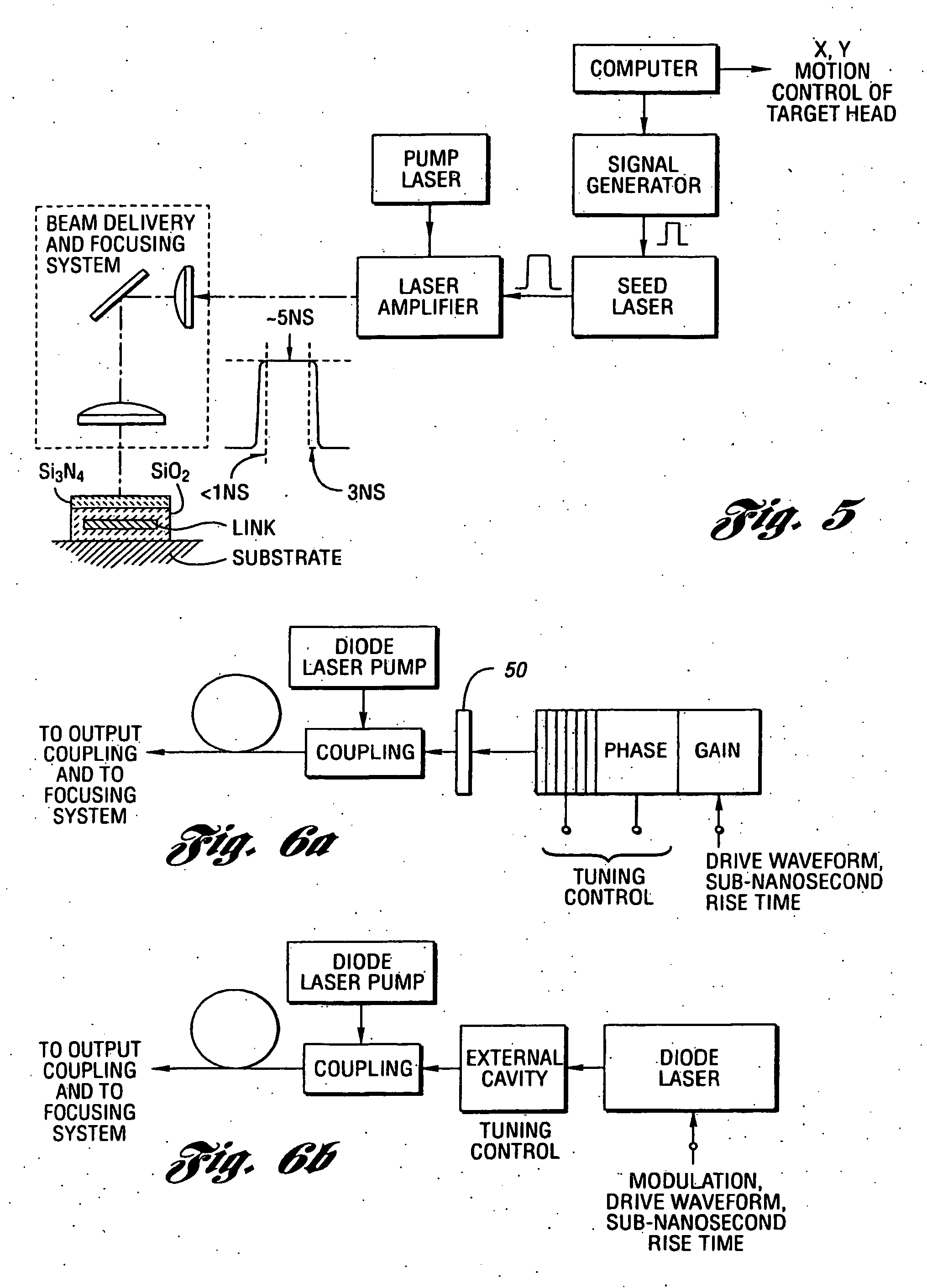
[0103] In a preferred embodiment of FIG. 7, a seed laser 10 and a fiber amplifier are mounted on a stable platform attached to the motion system 20 and the workpiece. It is very important in removing links that the beam be positioned with accuracy of less than 3 / 10 of a micron. The timing of the laser pulse to correlate with the relative positions of the target and optical system is important because of the continuous motion required in order to obtain high processing speeds.

[0104] The laser 10 is externally controlled by the computer 33 and a signal generator 11...


PUM

PropertyMeasurementUnit
Lengthaaaaaaaaaa
Fractionaaaaaaaaaa
Timeaaaaaaaaaa

Abstract

An energy-efficient method and system for processing target material such as microstructures in a microscopic region without causing undesirable changes in electrical and/or physical characteristics of material surrounding the target material is provided. The system includes a controller for generating a processing control signal and a signal generator for generating a modulated drive waveform based on the processing control signal. The waveform has a sub-nanosecond rise time. The system also includes a gain-switched, pulsed semiconductor seed laser for generating a laser pulse train at a repetition rate. The drive waveform pumps the laser so that each pulse of the pulse train has a predetermined shape. Further, the system includes a laser amplifier for optically amplifying the pulse train to obtain an amplified pulse train without significantly changing the predetermined shape of the pulses. The amplified pulses have little distortion and have substantially the same relative temporal power distribution as the original pulse train from the laser. Each of the amplified pulses has a substantially square temporal power density distribution, a sharp rise time, a pulse duration and a fall time. The system further includes a beam delivery and focusing subsystem for delivering and focusing at least a portion of the amplified pulse train onto the target material. The rise time (less than about 1 ns) is fast enough to efficiently couple laser energy to the target material, the pulse duration (typically 2-10 ns) is sufficient to process the target material, and the fall time (a few ns) is rapid enough to prevent the undesirable changes to the material surrounding the target material.

Description

CROSS REFERENCE TO RELATED PATENT AND APPLICATION [0001] This application is related to U.S. patent application Ser. No. 09 / 156,895, filed Sep. 18, 1998, entitled “High Speed Precision Positioning Apparatus”. This application is also related to U.S. Pat. No. 5,998,759 (i.e., the '759 patent) entitled “Laser Processing”, having the same assignee as the present invention. The entire disclosure of the '759 patent is hereby expressly incorporated by reference.TECHNICAL FIELD [0002] This invention relates to energy-efficient, laser-based methods and systems for processing target material. In particular, this invention relates to the use of a pulsed laser beam to ablate or otherwise alter a portion of a circuit element on a semiconductor substrate, and is particularly applicable to vaporizing metal, polysilicide and polysilicon links for memory repair. Further application can be found in laser-based micromachining and other repair operations, particularly when it is desired to ablate or m...

Claims


Application Information

Patent Timeline
IPC IPC(8): B23K26/16B23K26/06B23K26/00B23K26/064B23K26/073B23K26/40B23K101/36H01L21/302H01L21/768H01L23/525H01S3/00
CPCB23K26/063B23K26/0635B23K26/0736B23K26/365B23K26/4075Y10T29/49156H01L23/5258H01L2924/0002Y10S438/94H01L21/76894H01L2924/00B23K26/40B23K26/0622B23K26/0624B23K26/361B23K2103/50
Inventor SMART, DONALD V.
Owner ELECTRO SCI IND INC
Why Eureka
Try Eureka