Field effect transistor and its manufacturing method

a field effect transistor and manufacturing method technology, applied in the direction of basic electric elements, electrical appliances, semiconductor devices, etc., can solve the problems of compatibility of cost and productivity requested, slow performance of fet, and disadvantage in cost and productivity

Inactive Publication Date: 2006-05-25
HITACHI LTD
View PDF6 Cites 35 Cited by
  • Summary
  • Abstract
  • Description
  • Claims
  • Application Information

AI Technical Summary

Benefits of technology

[0018] Further, as in the invention, inorganic nanowires represented by silicon nanowire can be used, it is possible to realize TFT with carrier mobility of 10 to 100 times higher than TFT with channel of low-molecular-weight organic molecules or polymers. Thus, not only a device driving circuit but a peripheral circuit such as a shift register may be able to be made flexible.

Problems solved by technology

Generally, in case an organic molecules are used for a channel, a problem that the performance of FET is slow occurs.
However, the above-mentioned prior art has a problem from a viewpoint of the compatibility of the cost and the productivity requested from a practical viewpoint.
For example, as vacuum evaporation used in manufacturing a thin film of low-molecular-weight organics requires a vacuum though the vacuum evaporation has an advantage that the thin film having high carrier mobility can be easily formed, it is disadvantageous in the cost and the productivity.
Besides, the orientation of polymers and nanowires cannot be enhanced so much by reforming a surface on which a channel is formed or by rubbing, and carrier mobility cannot be enhanced to a required extent.
Propositions except these techniques also have a problem that the cost and the productivity cannot be also made compatible or enough orientation cannot be acquired.
Therefore, there is a problem that even if TFT can be manufactured at a low price, the display device cannot be driven or that even if the display device can be driven, a TFT manufacturing cost is high.

Method used


Image

  • Field effect transistor and its manufacturing method
  • Field effect transistor and its manufacturing method
  • Field effect transistor and its manufacturing method

Examples


first embodiment

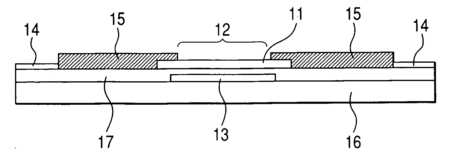
[0047]FIGS. 5A to 5E show a concrete example in which TFT according to the invention is formed using inorganic materials. In FIGS. 5A to 5E, sectional views are shown on the left and plans are shown on the right.

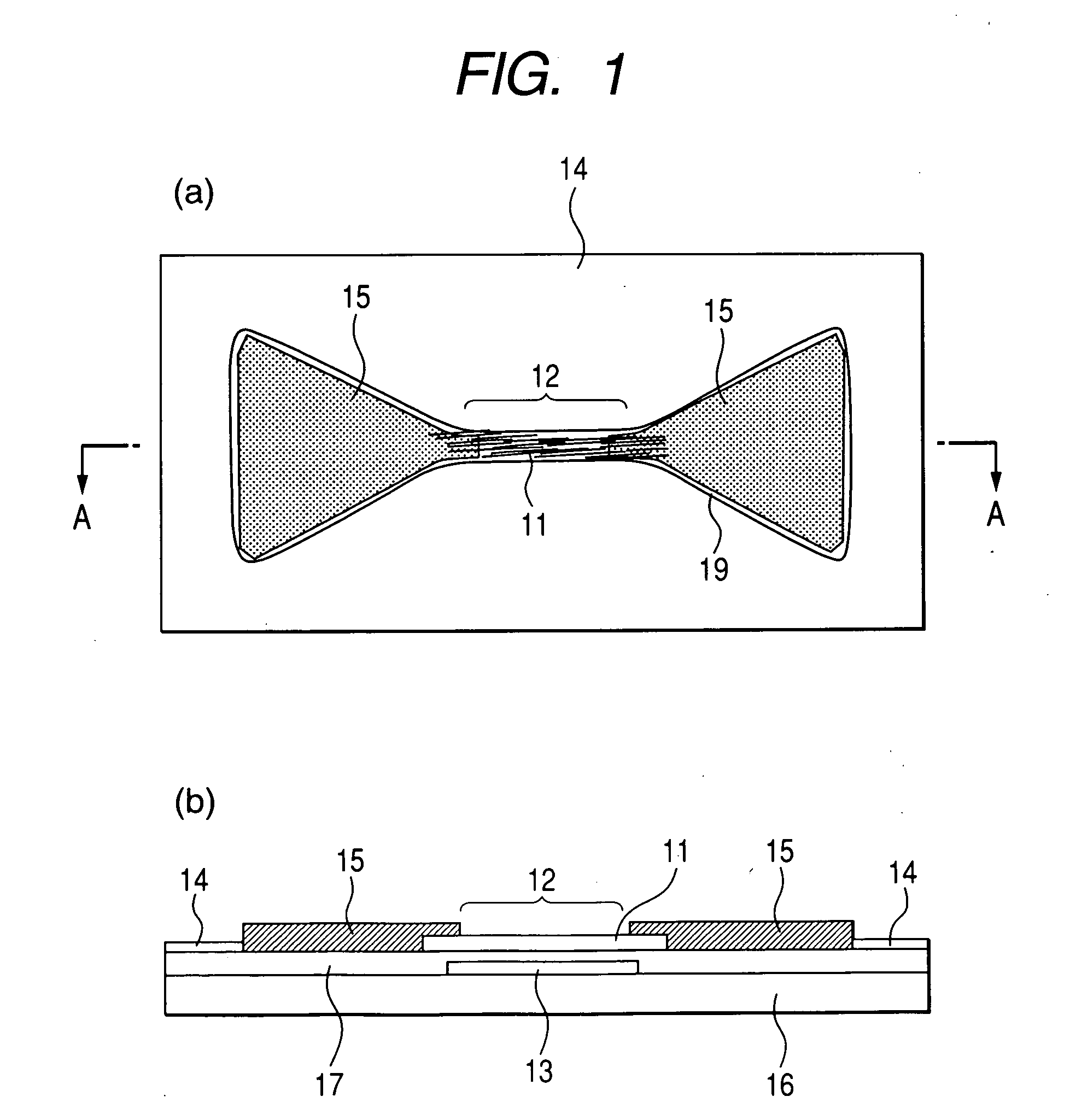
[0048] As shown in FIG. 5A, to form a gate electrode 13 on a silicon substrate 16, an aluminum thin film having the thickness of 30 nm is formed on a thermal oxide film 17 by sputtering evaporation. The gate electrode 13 is formed by forming the aluminum film in a pattern shown in the plan by photolithography. That is, in a first embodiment, TFT including the aggregate of narrow plural channels in the channel region shown in FIG. 3 is formed. In the first embodiment, the length of the gate electrode is set to 1 mm, the width of the narrow channel is set to 50 μm, and channel width is set to 5 mm as a whole.

[0049] Next, as shown in FIG. 5B, a silicon oxide insulator 51 having the thickness of 20 nm is formed by spurring evaporation. Further, resist is coated by a spin coat ...

second embodiment

[0059] In a second embodiment, a method of producing TFT which uses flexible materials for a substrate and an insulator and which does not use lithography in a low-priced way such as printing and application will be described.

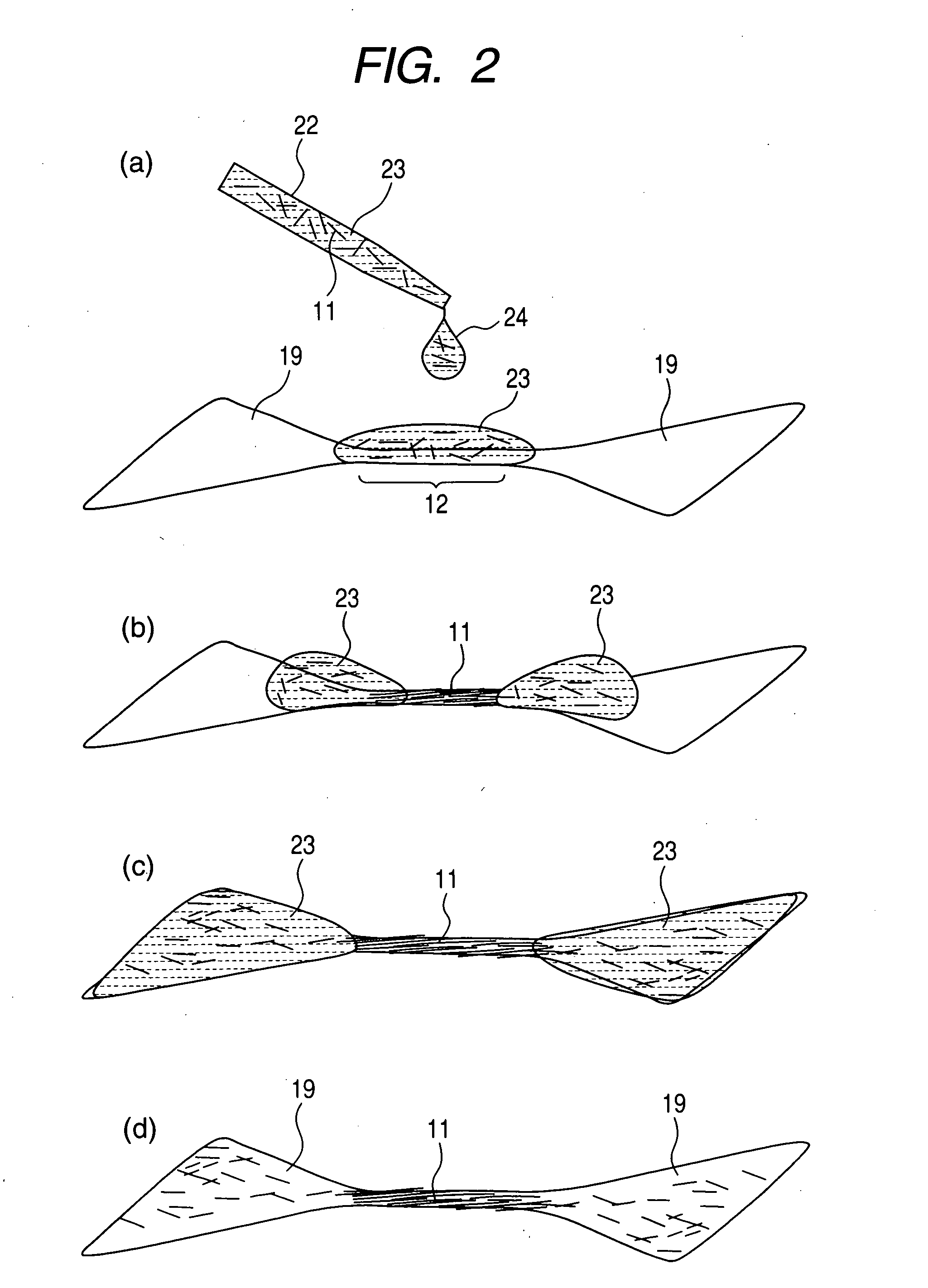
[0060] As in the method of forming the source and drain electrodes in the first embodiment, a gate electrode 13 having the pattern shown in FIG. 1A is printed on a plastic substrate using conducting ink. This is baked and the metal electrode 13 is formed; however, as plastic is used for the substrate, attention is required to be paid to softening temperature. In the second embodiment, a highly transparent polyimide sheet having the thickness of 100 μm is used for the substrate and as the baking temperature is set to approximately 300° C., it is verified that the substrate sufficiently endures the baking temperature of 120° C. in case water-based solution of silver nanoparticles is used. To form a gate insulator, polymethylmethacrylate (PMMA) is applied by a sp...

third embodiment

[0063] In a third embodiment, an example in which a pixel of an active matrix display device using TFT according to the invention for a driver circuit is manufactured will be described.

[0064]FIG. 6A shows an equivalent circuit for 3×3 pixels of the active matrix display device which uses TFTs of this invention in the driver circuit. A circuit for driving a pixel of a liquid crystal display cannot be used for a driver circuit for an organic electroluminescence device as it is as described on pp. 163 to 167 of the April 24 issue in 2000 of the Nikkei Electronics and one extra TFT is required for current control, compared with a liquid crystal. In this embodiment, a method of manufacturing a driver circuit which uses two TFTs per pixel will be described as described on pp. 163 to 167 of the April 24 issue in 2000 of the Nikkei Electronics and in JP-A No. 316295 / 2003.

[0065] A reference number 618 denotes a driver circuit for scan lines and the driver circuit sends a signal to the scan...


PUM


Abstract

To provide a method of easily producing TFT in which the orientation of channel molecules or wires is enhanced, compared with conventional type organic TFT at a low price, a lyophilic TFT pattern encircled by a lyophobic area is formed on a substrate, spontaneous movement is made in a droplet containing organic molecules or nanowires dropped in a channel region by characterizing the form of the pattern, and the organic molecules or the nanowires are oriented in the channel region by the movement.

Description

CLAIM OF PRIORITY [0001] The present application claims priority from Japanese application JP 2004-335779 filed on Nov. 19, 2004, the contents of which are hereby incorporated by reference into this application. FIELD OF THE INVENTION [0002] The present invention relates to a method of manufacturing a transistor, particularly relates to a method of manufacturing a transistor characterized in structure in which a channel of a transistor is formed by the aggregate of one-dimensional structures and the one-dimensional structures are highly oriented substantially in parallel with the channel between so-called two source and drain electrodes. BACKGROUND OF THE INVENTION [0003] In a thin, flat display device such as a liquid crystal display or an organic electroluminescent (EL) display, thin film transistors (TFT) using amorphous silicon or polycrystalline silicon for the material of a channel is used for a picture element driving device. In the meantime, as for a display device using an ...

Claims


Application Information

Patent Timeline
Patent Type & Authority Applications(United States)
IPC IPC(8): H01L51/40H01L21/84H01L21/00
CPCH01L51/0003H01L51/0012H01L51/0541H01L51/0545H10K71/191H10K71/12H10K10/464H10K10/466
Inventor FUJIMORI, MASAAKIHASHIZUME, TOMIHIROANDO, MASAHIKO
Owner HITACHI LTD
Why Eureka
Try Eureka