Memory element and memory device

a memory element and memory technology, applied in the field of memory elements, can solve the problems of inability to obtain high speed operation of memory elements, and achieve the effects of preventing further deterioration of memory elements, enhancing reliability of memory elements, and maintaining stably

Active Publication Date: 2006-06-15
SONY CORP
View PDF1 Cites 74 Cited by
  • Summary
  • Abstract
  • Description
  • Claims
  • Application Information

AI Technical Summary

Benefits of technology

[0046] Accordingly, even in the case where the resistance value of the ion source layer including CuTe is changed due to rise in temperature, which has little effect on the change in the resistance value of the memory element, operation of a memory may not be affected considerably.
[0047] Consequently, deterioration of characteristics of the memory element can further be prevented, when the memory element is manufactured, used, and retained under a high-temperature environment.
[0048] According to the above-described embodiments of the present invention, since the state of high resistance can be maintained stably even if the memory eleme

Problems solved by technology

It is assumed that the problem of the resistance value being an intermediate value is caused by the fact that the thickness of a thin film made of Ges, Gese and the like, in which resistance is changed, is comparatively thick (10 nm or more, for example) and so an electric field generated when a voltage is applied becomes comparatively wea

Method used


Image

  • Memory element and memory device
  • Memory element and memory device
  • Memory element and memory device

Examples


experiment 1

[Experiment 1]

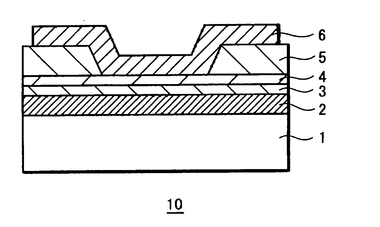
[0123] On a silicon wafer, a tantalum (Ta) film of 20 nm in thickness was deposited as the lower electrode 2, a Cu50Te35Ge15 film of 20 nm in thickness was formed thereon as the ion source layer 3, an oxide tantalum film was formed as the memory thin film 4 and photoresist was formed to cover the surface, and after that, exposure and development were performed by means of photolithography to form an opening (through hole) in the photoresist on the memory thin film 4. Among those layers, the oxide tantalum film was formed such that after a tantalum film in the metal state was formed in the thickness of 1 nm by sputtering, oxidation treatment was performed in oxygen contained plasma atmosphere. It is assumed that the oxide tantalum film became somewhat thicker than the original tantalum film by the above oxidation treatment.

[0124] Subsequently, annealing treatment was performed in a vacuum and the photoresist was transformed to be the insulation layer 5 as hard-cured re...

experiment 2

[Experiment 2]

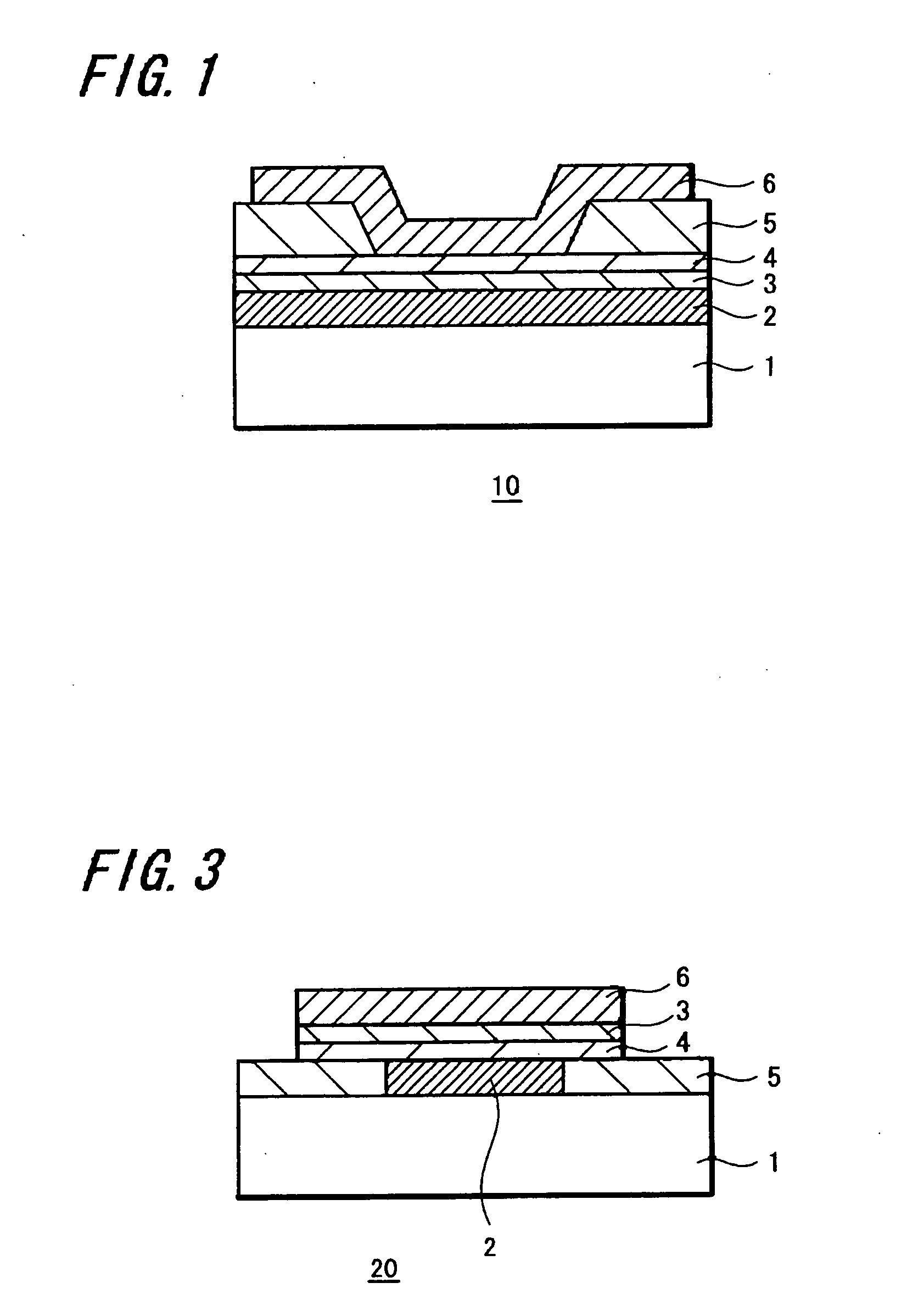
[0138] Instead of the memory element 10 shown in FIG. 1, a memory element 20 shown in FIG. 3 was manufactured as another embodiment of the present invention and the characteristic thereof was studied.

[0139] In the memory element 20 shown in FIG. 3, the memory thin film (memory layer) 4 was formed below the ion source layer 3, on the contrary to the memory element 10 shown in FIG. 1 according to the previous embodiment. Further, the upper electrode 6 was made of the same pattern as the memory thin film 4 and ion source layer 3. The lower electrode 2 was made of a smaller pattern and was buried in an opening formed in the insulation film 5.

[0140] Similarly to the memory element 10 according to the previous embodiment, since the memory thin film 4 (memory layer) 4 in the memory element 20 shown in FIG. 3 is made of the above-described oxide film, the thermal resistance of the memory thin film (memory layer) 4 is improved, a yield ratio of manufacturing the memory elemen...

experiment 3

[Experiment 3]

[Repeated Recording and Erasure Experiments]

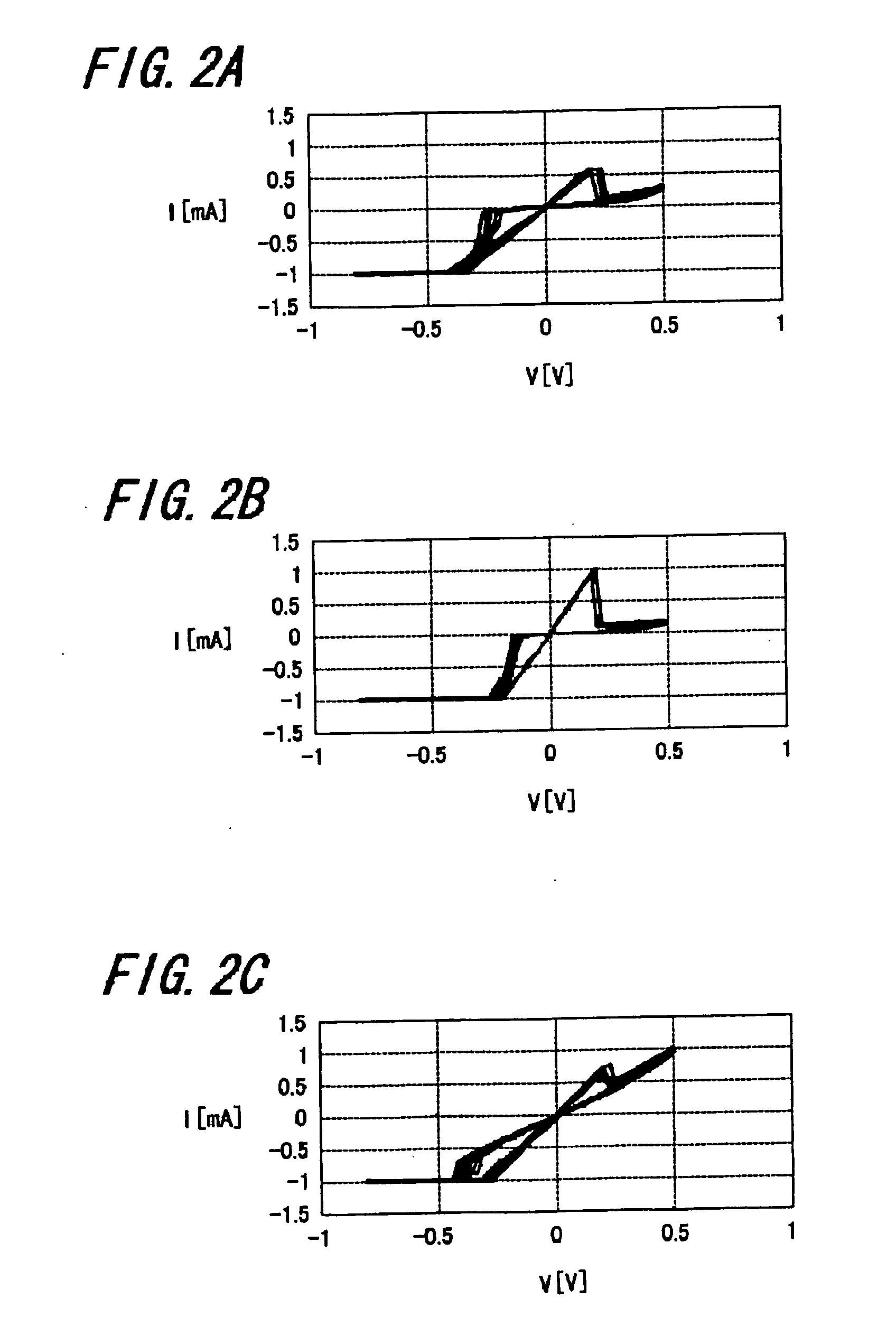
[0162] Next, a measuring apparatus was constructed as shown in FIG. 8 with respect to a sample of the memory element 20 similar to the one used in the experiment 2, and the recording and erasure experiments were repeatedly performed.

[0163] The measuring apparatus shown in FIG. 8 includes an arbitrary waveform generator 31 and a digital oscilloscope 32.

[0164] The arbitrary waveform generator 31 was connected to the load resistance enclosed by a broken line through a pulse applying line 33. Further, the digital oscilloscope 32 was connected to the load resistance through two voltage monitor lines 34. The load resistance had two lines of the resistance value 50 Ω and of the resistance value RL (2 kΩ).

[0165] Further, wiring was connected from the load resistance to the substrate of the wafer 35 (rear surface side) and to the upper electrode side, respectively.

[0166] Using the above-described measuring apparatus, a recording ...


PUM


Abstract

A memory element which stably performs operations such as data recording and which has a stable structure with respect to heat is provided.
A memory element 10 includes a memory layer 4 and an ion source layer 3 positioned between the first electrode 2 and second electrode 6, in which the ion source layer 3 contains any of elements selected from Cu, Ag and Zn, and any of elements selected from Te, S and Se, and the memory layer 4 is made of any of tantalum oxide, niobium oxide, aluminum oxide, hafnium oxide and zirconium oxide, or is made of mixed materials thereof.

Description

CROSS REFERENCES TO RELATED APPLICATIONS [0001] The present invention contains subject matter related to Japanese Patent Application JP 2004-361755 in the Japanese Patent Office on Dec. 14, 2004, the entire contents of which being incorporated herein by reference. BACKGROUND OF THE INVENTION [0002] 1. Field of the Invention [0003] The present invention relates to a memory element in which data can be recorded and a memory device including the memory element. [0004] 2. Description of the Related Art [0005] In information devices such as a computer, a DRAM capable of high speed operation and having high density is used as a random access memory. [0006] However, since the DRAM has a complicated manufacturing process compared with a typical logic circuit LSI and signal processing employed in an electronic apparatus, manufacture costs increase. [0007] Further, since the DRAM is a volatile memory in which data disappears when the power is shut off, such refreshing operation that data writ...

Claims


Application Information

Patent Timeline
IPC IPC(8): G11C8/02
CPCG11C13/0007G11C2213/31G11C2213/56H01L45/1625H01L45/085H01L45/1233H01L45/1266H01L45/146H10N70/245H10N70/8416H10N70/826H10N70/8833H10N70/026H01L27/10
Inventor ARATANI, KATSUHISAKOUCHIYAMA, AKIRAMIZUGUCHI, TETSUYA
Owner SONY CORP
Why Eureka
Try Eureka